Transparent, electrically conductive layer, a process for producing the layer and its use

Inactive Publication Date: 2008-09-25
EVONIK DEGUSSA GMBH
View PDF13 Cites 19 Cited by
  • Summary
  • Abstract
  • Description
  • Claims
  • Application Information

AI Technical Summary

Problems solved by technology

However, this process has the disadvantage of an unsatisfactorily low transmission of the layer, which is between 79% and 82%.
However, this is much more complicated from a technical point of view and is therefore too expensive for commercial applications.
Since an nonconductive organic binder which enables a certain unspecified mechanical stability of the layer is used in U.S. Pat. No. 6,511,614, the specific resistance at over 0.1 Ω·cm is much too high to obtain highly conductive layers.
The layers obtained in this way are, however, highly porous.
The use of such great layer thicknesses in modem displays is, however, technically disadvantageous and economically unviable.
A further disadvantage of particulate layers is the low mechanical stability which, as a result of the sintering of the particles with one another and with the support material, is so weak that the layers can be wiped readily off the carrier.
Since the common polymers are, however, p-conductive, while most of and the best conductive metal oxides are n-conductive, these materials are generally incompatible.
These values are too high for applications in displays or photovoltai

Method used


Image

  • Transparent, electrically conductive layer, a process for producing the layer and its use
  • Transparent, electrically conductive layer, a process for producing the layer and its use
  • Transparent, electrically conductive layer, a process for producing the layer and its use

Examples


examples

General Techniques

[0113]All syntheses involving organometallic compounds were effected, owing to their high air and moisture sensitivity, in a protective gas atmosphere composed of nitrogen which was available through evaporation of liquid nitrogen (Messer Griesheim). All reactions were effected with the aid of standard Schlenk techniques or in a glovebox.

[0114]Before utilization under reduced pressure, the glass apparatus used was baked out with a naked flame and, after cooling, filled with nitrogen and evacuated three times. Only after this operation was the filling of chemicals commenced. Liquid substances were transferred by means of syringes and cannula which were stored in a drying cabinet and flushed repeatedly with nitrogen before use.

[0115]In the syntheses, only anhydrous chemicals were used. The solvents used were dried by standard methods: tetrahydrofuran, diethyl ether, toluene, n-pentane and n-hexane were absoluted with sodium and benzophenone in the protective atmosphe...


PUM

PropertyMeasurementUnit
Thicknessaaaaaaaaaa
Thicknessaaaaaaaaaa
Transparencyaaaaaaaaaa

Abstract

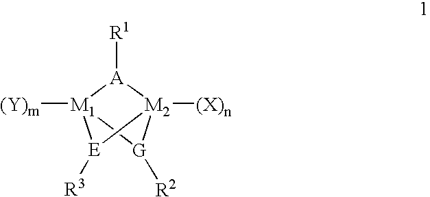
Transparent, electrically conductive layer, a process for producing the layer and its use, wherein the layer is based on at least one compound of the formula 1
wherein the substituents are as defined.

Description

BACKGROUND OF THE INVENTION[0001]1. Field of the Invention[0002]The present invention relates to a transparent, electrically conductive layer, to a process for producing the layer and to its use.[0003]2. Description of the Background[0004]Transparent layers with high ohmic conductivity have areal resistances of at most 1000 μ□ and a transmission of over 70% and are required in all modem displays, for example in LCDs, plasma displays, OLEDs, and, for example, also in organic solar cells, in order to be able to utilize the electrically currents excited by the photovoltaic effect with low losses.[0005]A mechanically stable layer is understood hereinafter to mean a layer which has resistance to stress by scratching, sharp-edged objects or materials, characterized, for example, by the pencil hardness according to DIN EN 13523-4:2001.[0006]Areal resistance is understood hereinafter to mean the ohmic resistance which is obtained on a coating with a uniform coating thickness when a square r...

Claims


Application Information

Patent Timeline
IPC IPC(8): B32B9/04B05D3/00B32B15/00B32B17/06C07F5/00C07F7/22C07F19/00B32B27/32B32B27/36
CPCC03C17/002Y10T428/24802C03C17/3417C03C2217/231C03C2218/11C03C2218/15C23C18/1216C23C18/1279C23C18/1295C23C18/14H01B1/08H01L51/442H01L51/5203H01L2251/308C03C17/253Y10T428/31935Y10T428/31725Y10T428/249921Y10T428/31678Y10T428/31938Y10T428/31993Y10T428/31989Y10T428/31504Y10T428/31507C23C18/143C23C18/145H10K30/82H10K50/805H10K2102/103
Inventor LUTHGE, THOMASFUGEMANN, RITAINHESTER, MARTINADRIESS, MATTHIASAKSU, YILMAZ
Owner EVONIK DEGUSSA GMBH
Why Eureka
Try Eureka