
Photosensitive Composition, Pattern Forming Material, Photosensitive Laminate, Pattern Forming Apparatus, and Pattern Forming Process

a technology of composition and pattern forming, which is applied in the direction of photosensitive materials for photomechanical equipment, microlithography exposure equipment, photosensitive materials, etc., can solve the problems of power output and wavelength uniformity that are far from satisfactory, and cannot allow for differences in spectral sensitivity, so as to prevent variations in pattern form and reproductivity. , the effect of constant photosensitivity distribution

Inactive Publication Date: 2008-10-30
ASAHI KASEI E-MATERIALS CORPORATION
View PDF0 Cites 33 Cited by
  • Summary
  • Abstract
  • Description
  • Claims
  • Application Information

AI Technical Summary

Benefits of technology

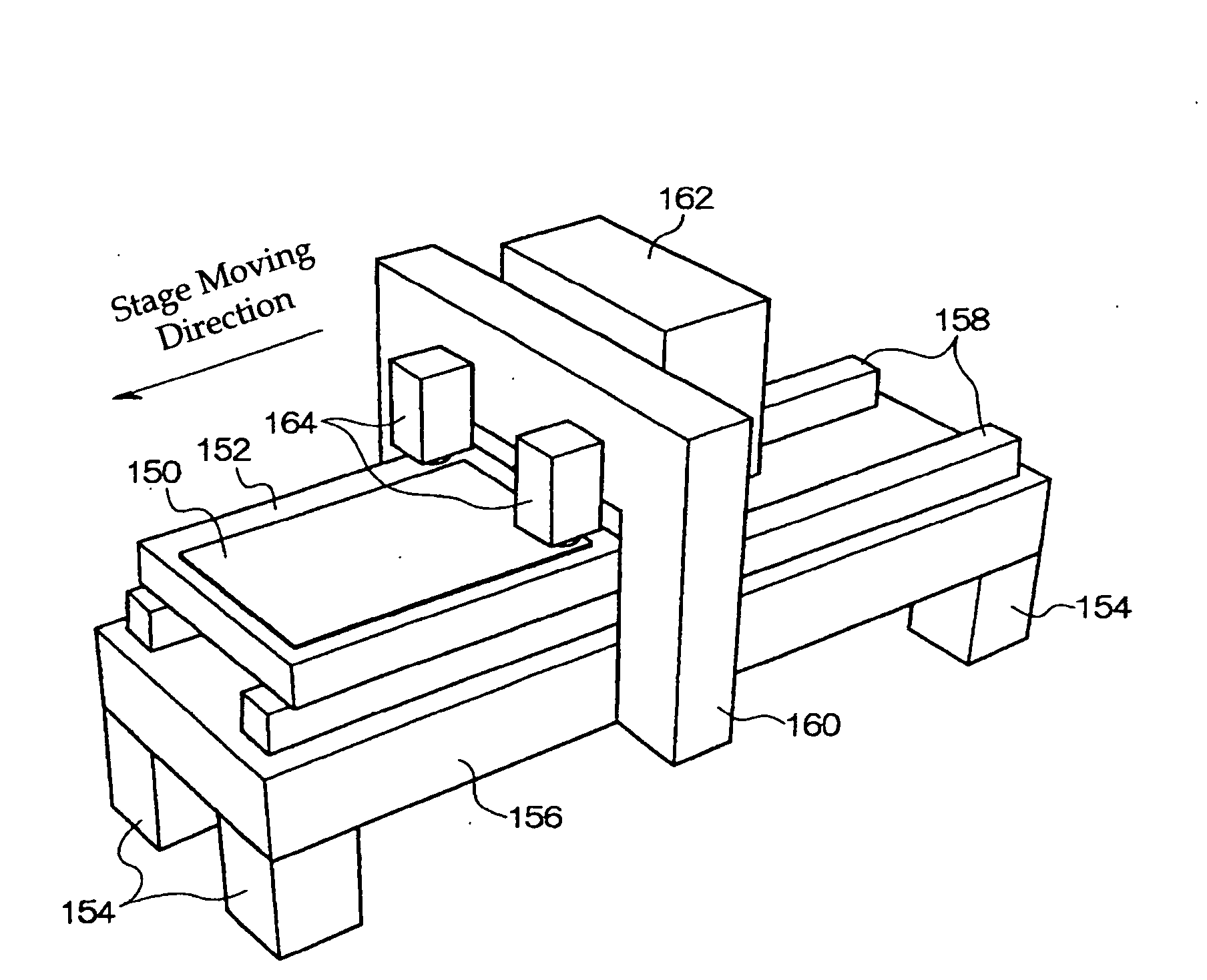
[0058]In the pattern forming apparatus according to the item <45>, the light irradiation unit allowing for combining two or more types of light for irradiation enables exposures with deeper focal depth. As the result, the photosensitive layer can be finely and precisely exposed.
[0060]In the pattern forming apparatus according to the item <46>, the light irradiation unit can collect laser beams respectively emitted from the plural lasers by the use of the collecting optical system and connect them to the multimode optical fiber, and thus it enables exposures with deeper focal depth. As the result, the photosensitive layer can be finely and precisely exposed.
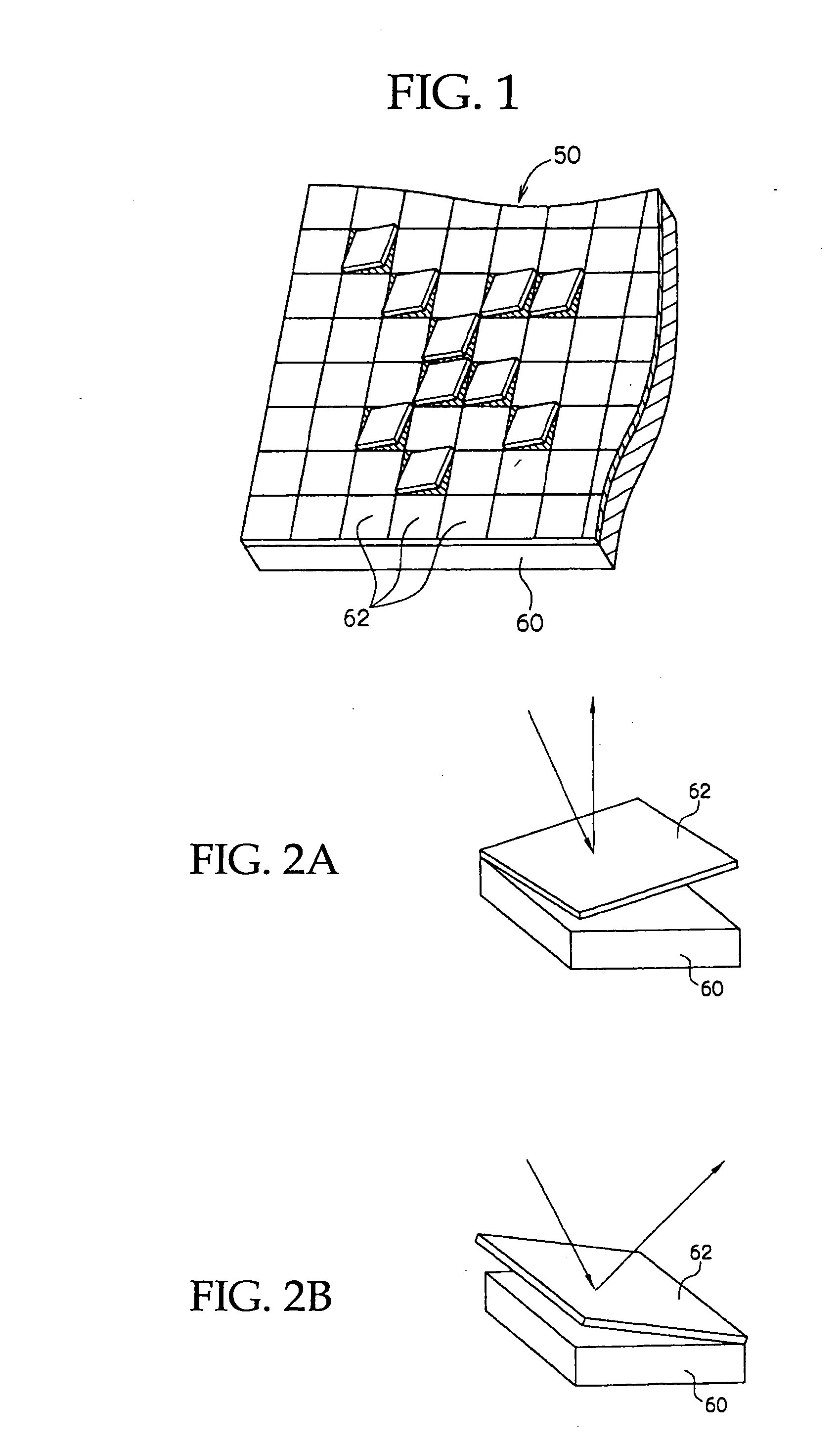
[0070]In the pattern forming process according to the item <54>, the light beam modulated by the light modulating unit passes through the non-spherical surface in the microlens array. With this configuration, the aberration due to distortion at irradiating surface of the imaging portion can be compensated. As the result, distortion of an image to be formed on the pattern forming material is prevented, and the photosensitive layer can be finely and precisely exposed.
[0072]In the pattern forming process according to the item <55>, the non-spherical surface is a toric surface, and thus aberration due to distortion at irradiating surface of the imaging portion can be efficiently compensated, and distortion of an image to be formed on the pattern forming material can be efficiently prevented. As the result, the photosensitive layer can be finely and precisely exposed.
[0074]In the pattern forming process according to the item <56>, the photosensitive layer is exposed through an aperture array, and thus the extinction ratio is increased. As the result, the photosensitive layer can be finely and precisely exposed.
[0086]The present invention can solve the above-noted conventional problems and can provide a photosensitive composition which has an extremely constant photosensitivity distribution relative to an exposure light having a wavelength in the region of short-wavelengths (blue-violet light), in particular, having a wavelength of 400 nm to 410 nm, is excellent in pattern reproductivity without being affected by variations in exposure wavelength during exposure with a laser beam, and allows substantially preventing variations in form of patterns as well as allows for easy handling under bright room environments. The present invention can also provide a pattern forming material and a photosensitive laminate each of which the photosensitive composition is formed in a laminate structure, a pattern forming apparatus, a pattern forming process, and highly fine and precise interconnection patterns and permanent patterns such as protective insulating films, and solder resist patterns.

Problems solved by technology

As developments of lasers which can stably oscillate in the region of short-wavelengths (blue-violet light) expands, the lasers started to be utilized as exposure light sources, however, the power output and the uniformity of the wavelengths are far from satisfactory.
In the meanwhile, in an exposing unit in which a plurality of exposure heads are arrayed to expose a photosensitive material, when there are variations in wavelength of an irradiation light attributable to variations of a semiconductor device serving as an irradiation light source, the uniformity of the formed pattern is impaired because the exposed photosensitive material reacts differently and with different sensitivities depending on the spectral sensitivity for every different regions in the photosensitive material which are exposed with different exposure wavelengths.
However, the above-noted proposal does not allow for difference in spectral sensitivity relative to a certain wavelength region centering on the wavelength of an exposure light, and does not disclose a solution to the difference in wavelength depending on an exposure light source, by means of the spectral sensitivity of the photosensitive material.
Further, the proposal has a problem that a sufficient sensitivity is not assured when a solid laser having a wavelength of 405 nm, which has been widely used in recent years, is used as an exposure light source.

Method used


Image

  • Photosensitive Composition, Pattern Forming Material, Photosensitive Laminate, Pattern Forming Apparatus, and Pattern Forming Process
  • Photosensitive Composition, Pattern Forming Material, Photosensitive Laminate, Pattern Forming Apparatus, and Pattern Forming Process
  • Photosensitive Composition, Pattern Forming Material, Photosensitive Laminate, Pattern Forming Apparatus, and Pattern Forming Process

Examples


example 1

Preparation of Pattern Forming Material for Dry Film Resist

[0687]Over a surface of a polyethylene terephthalate film having a thickness of 20 μm serving as the support set forth, a photosensitive composition solution for dry film resist was applied, and the surface of the support was dried to form a photosensitive layer having a thickness of 15 μm on the support, thereby preparing the above-noted pattern forming material for dry film resist.

[Composition of Photosensitive Composition for Dry Film Resist]Methyl methacrylate / styrene / benzyl60parts by massmethacrylate / methacrylic acid copolymer(copolymer composition (mass ratio):8 / 30 / 37 / 25; mass averagemolecular mass: 60,000; acid value: 163)Polymerizable monomer represented by7.0parts by massthe following formula (75)Adduct between hexamethylene7.0parts by massdiisocyanate and tetraethylene oxidemonomethacrylate (molar ratio: 1 / 2)N-methylacridone0.11parts by mass2,2-bis(o-chlorophenyl)-4,4′,5,5′-2.17parts by masstetraphenylbiimidazoleN-...

example 2

[0700]A pattern forming material for dry film resist and a photosensitive laminate for dry film resist were produced in the same manner as in Example 1 except that N-methyl acridone in the photosensitive composition solution for dry film resist was changed to 10-N-butyl-2-chloroacridone. The maximum absorption wavelength of 10-N-butyl-2-chloroacridone as the above-noted photosensitizer was 365 nm.

[0701]With respect to the pattern forming material for dry film resist and the photosensitive laminate, the shortest developing time, the spectral sensitivity, and the minimum exposure dose capable of forming a pattern were measured in the same manner as in Example 1. Further, variations in line width of the formed lines were measured in the same manner as in Example 1. Table 3 shows the measurement results. The shortest developing time was 7 seconds.

example 3

[0702]A pattern forming material for dry film resist and a photosensitive laminate for dry film resist were produced in the same manner as in Example 1 except that the content of 2,2-bis(o-chlorophenyl)-4,4′,5,5′-tetraphenylbiimidazole was changed to 0.50 parts by mass.

[0703]With respect to the pattern forming material for dry film resist and the photosensitive laminate, the shortest developing time, the spectral sensitivity, and the minimum exposure dose capable of forming a pattern were measured in the same manner as in Example 1. Further, variations in line width of the formed lines were measured in the same manner as in Example 1. Table 3 shows the measurement results. The shortest developing time was 7 seconds.


PUM

PropertyMeasurementUnit
wavelength rangeaaaaaaaaaa
wavelengthaaaaaaaaaa

Abstract

A photosensitive composition having an extremely constant photosensitivity distribution relative to an exposure light having a wavelength of 400 nm to 410 nm, and excelling in pattern reproductivity, suppressing variations in pattern formation; a pattern forming material and a photosensitive laminate with the photosensitive composition laminated thereon; and a pattern forming apparatus and a pattern forming process.The photosensitive composition contains a binder, a polymerizable compound, and a photopolymerization initiator; the photosensitive composition has a maximum spectral sensitivity in the wavelength range of 380 nm to 420 nm; the minimum exposure dose S400 capable of forming a pattern at a wavelength of 400 nm of the photosensitive composition is 300 mJ / cm2 or less; the minimum exposure dose S410 capable of forming a pattern at a wavelength of 410 nm of the photosensitive composition is 300 mJ / cm2 or less; and S400 and S410 satisfy the relation 0.6<S400 / S410<1.6.

Description

TECHNICAL FIELD[0001]The present invention relates to a photosensitive composition preferably used for dry film resist (DFR), solder resist, liquid solder resist, and the like which are capable of forming images by means of UV exposure. In particular, the present invention relates to a pattern forming material and a photosensitive laminate using the photosensitive composition, a pattern forming apparatus provided with the pattern forming material and the photosensitive laminate, a pattern forming process using the pattern forming material and the photosensitive laminate as well as interconnection patterns and permanent patterns such as protective layers, interlayer insulating films, and solder resist patterns.BACKGROUND ART[0002]When producing a printed wiring board, first, a dry film resist (DFR) is used for a copper clad laminate to form a copper interconnection pattern. Further, various parts such as semiconductors, capacitors, and resistors are soldered on the printed wiring boa...

Claims


Application Information

Patent Timeline
Patent Type & Authority Applications(United States)
IPC IPC(8): G03F7/20G03C1/00
CPCG03F7/0045G03F7/028G03F7/031G03F7/0295G03F7/029G03F7/004G03F7/0047G03F7/20G03F7/202G03F7/027
Inventor TASHIRO, TOMOKOSATO, MORIMASASASAKI, YOSHIHARUWAKATA, YUICHITAKAYANAGI, TAKASHI
Owner ASAHI KASEI E-MATERIALS CORPORATION
Learn More