Charge-transporting varnishes containing charge-transporting polymers and organic electroluminescent devices made by using the same

a charge-transporting polymer and varnish technology, applied in the direction of discharge tube/lamp details, discharge tube luminescnet screens, electrically-conductive paints, etc., can solve the problems of low mechanical strength and heat resistance, device with lowered characteristics, and uneven surface, so as to prevent electric short-circuiting, excellent mechanical strength, and high uniformity and flatness

Inactive Publication Date: 2009-03-05
NISSAN CHEM IND LTD
View PDF14 Cites 7 Cited by
  • Summary
  • Abstract
  • Description
  • Claims
  • Application Information

AI Technical Summary

Benefits of technology

[0019]The use of the charge-transporting varnish of the invention makes it possible to form charge-transporting thin films of high uniformity and flatness and excellent mechanical strength, heat resistance and transparency by various methods, such as spin coating, printing, spraying and the like.
[0020]By forming a charge-transporting thin film according to the invention on an electrode surface, the electrode surface is rendered flat and uniform so that electric short-circuiting can be prevented. The use of these thin films as a charge injection layer and a charge transport layer in an organic EL device makes it possible to realize improvements in initial characteristics and an increase in device operating life, such as lower drive voltage and higher luminescence efficiency.
[0021]The charge-transporting varnish of the invention has high self-flattening property and heat resistance and can easily form charge-transporting thin films by various coating methods, and therefore, is useful for applications in organic electronic devices such as organic field-effect devices, as capacitor-electrode protecting films, and also as antistatic films.

Problems solved by technology

The film so formed is, however, accompanied by a drawback that its surfaces are markedly uneven and its material hence mixes in trace amounts in other organic layers to provide the resulting device with lowered characteristics.
However, thin films formed with varnishes dispersed in organic solvents involve drawbacks that they have low mechanical strength and poor heat resistance.
Moreover, the removal of a solvent tends to produce powder so that problems are developed in the uniformity and flatness of thin films.

Method used


Image

  • Charge-transporting varnishes containing charge-transporting polymers and organic electroluminescent devices made by using the same
  • Charge-transporting varnishes containing charge-transporting polymers and organic electroluminescent devices made by using the same
  • Charge-transporting varnishes containing charge-transporting polymers and organic electroluminescent devices made by using the same

Examples


synthesis example 1

Synthesis of Oligoaniline

[0121]Based on the procedure descried in Bulletin of Chemical Society of Japan, 67, p. 1749 to 1752, 1994, phenyltetraaniline (PTA) was obtained as will be described hereinafter.

[0122]p-phenylenediamine (12.977 g) was dissolved in toluene (2 liters), and in the resultant solution, tetra-n-butoxy titanium (245.05 g) was added and dissolved at 70° C. for 30 minutes. To the thus-prepared solution, p-hydroxydiphenylamine (53.346 g) was then added, followed by a reaction under a nitrogen atmosphere at a reaction temperature of 100° C. for 24 hours. Subsequent to the completion of the reaction, the reaction mixture was filtered, the filter cake was successively washed with toluene and ethyl ether and then dried to obtain silvery crystals. To the thus-obtained crystals, dioxane (25 parts) and hydrazine monohydrate (0.2 equivalent) were added. After the interior of the reaction system was purged with nitrogen, the reaction mixture was heated under reflux to dissolve...

synthesis example 2

Polymerization of Polyamic Acid (PI-x1)

[0123]Under a nitrogen gas stream, N,N′-diphenyl-N,N′-di-(4-aminophenoxy)phenyl)benzidine (hereinafter abbreviated as “TPD-DA”) (3.51 g, 5.0 mmol) was placed in a 100 mL four necked flask, and subsequent to its dissolution in NMP (10.0 g), a suspension of 1,2,3,4-cyclobutanetetracarboxylic anhydride (hereinafter abbreviated as “CBDA”; 0.91 g, 4.6 mmol) in NMP (15.1 g) was added. The resulting mixture was stirred at 23° C. for 6 hours to conduct a polymerization reaction, whereby a 15% NMP solution of a polyamic acid (PI-x1) as a polyimide precursor was obtained. The number average molecular weight (Mn) and weight average molecular weight (Mw) of the thus-obtained polyamic acid (PI-x1) were Mn=17,300 and Mw=35,800, respectively.

synthesis example 3

Polymerization of Polyamic Acid (PI-x2)

[0124]Under a nitrogen gas stream, TPD-DA (1.69 g, 2.4 mmol) and p-phenylenediamine (1.03 g, 9.6 mmol) were placed in a 100 mL four necked flask, and subsequent to their dissolution in NMP (12.0 g), a suspension of CBDA (2.26 g, 11.5 mmol) in NMP (32.8 g) was added. The resulting mixture was stirred at 23° C. for 6 hours to conduct a polymerization reaction, whereby a 10% NMP solution of a polyamic acid (PI-x2) as a polyimide precursor was obtained. The number average molecular weight (Mn) and weight average molecular weight (Mw) of the thus-obtained polyamic acid (PI-x2) were 53,000 and Mw=122,000, respectively.

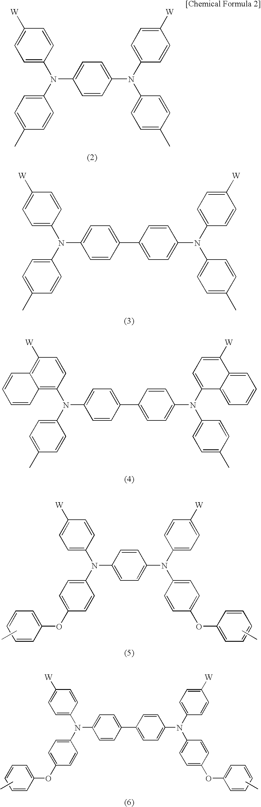
[0125]It is to be noted that TPD-DA used in the above-described Synthesis Examples 2 and 3 and represented by the following formula was synthesized following the procedure described in the pamphlet of PCT International Publication No. WO 02 / 100949.


PUM

PropertyMeasurementUnit
drive voltageaaaaaaaaaa
temperatureaaaaaaaaaa

Abstract

A charge-transporting varnish comprising a solution or dispersion of at least one charge-transporting polymer comprising repeating units represented by the general formula (1) in at least one solvent, wherein the polymer is at least one polymer selected from among polyimide precursors having number-average molecular weights of 1,000 to 100,000 and polyimides obtained by cyclodehydration of the precursors; a charge-transporting varnish comprising a solution or dispersion in at least one solvent of both a charge-transporting substance consisting of a charge-transporting oligoaniline derivative having a number-average molecular weight of 250 to 5,000 or a charge-transporting organic material consisting of the substance and a charge-receiving dopant and at least one charge-transporting polymer comprising repeating units represented by the general formula (1); charge-transporting thin films formed by using the varnishes; and organic electroluminescent devices provided with the thin films: (1) wherein Ar1 to Ar3 are each independently monovalent aryl; Ar4 to Ar7 are each independently divalent aryl; X1 and X2 are each independently a divalent organic group; X3 and X4 are each independently a single bond, —O—, —S—, —C(O)NH—, —NHC(O)—, imino which may be substituted with a monovalent hydrocarbon group, alkylene of 1 to 5 carbon atoms which may have a branched structure, or alkylenedioxo of 1 to 5 carbon atoms which may have a branched structure; n is 0 or a positive integer of 3 or below; and i and j are each independently 0 or 1.

Description

TECHNICAL FIELD[0001]This invention relates to charge-transporting varnishes containing charge-transporting polymers and organic electroluminescent devices (hereinafter abbreviated as “EL”) making use of the same.BACKGROUND ART[0002]Since the finding of an organic EL device, which showed a characteristic property of 1,000 cd / m2 or so at a drive voltage of 10 V or lower, by Tang et al. of Eastman Kodak Company in 1987 (see, for example, Non-Patent Document 1), active investigations have been made on organic EL devices. These organic EL devices can be roughly divided into low-molecular organic EL devices (hereinafter abbreviated as “OLED”) and EL devices making use of polymer light-emitting materials (hereinafter abbreviated as “PLED”. In general, both OLED and PLED use a hole injection layer and a hole transport layer to achieve improvements in initial characteristics and an increase in device operating life, such as lower drive voltage and higher luminescence efficiency.[0003]As CuP...

Claims


Application Information

Patent Timeline
Patent Type & Authority Applications(United States)
IPC IPC(8): C08G73/04H01J1/63
CPCC08G73/024C08G73/026C09D5/24C09D179/08H01L51/0035H01L51/5048H01L51/0039H01L51/0081C08L2666/20H10K85/111H10K85/115H10K85/324H10K50/14C09D201/00C09D179/00
Inventor ONO, GOYAMADA, TOMOHISA
Owner NISSAN CHEM IND LTD
Why Eureka
Try Eureka