
Display device

a display device and top emission technology, applied in the direction of discharge tube luminescnet screens, organic semiconductor devices, discharge tube/lamp details, etc., can solve the problems of easy damage to the base reflective layer, etching residue or the like, and the cost of the polishing process, so as to reduce the number of processes, prevent the effect of reducing the manufacturing yield and reducing the manufacturing cos

Inactive Publication Date: 2009-03-05
HITACHI DISPLAYS
View PDF4 Cites 24 Cited by
  • Summary
  • Abstract
  • Description
  • Claims
  • Application Information

AI Technical Summary

Benefits of technology

[0009]As heretofore described, with the top emission type organic electroluminescent display device anode, a transparent conduction film, such as indium tin oxide or indium zinc oxide, is formed on a reflective layer. In this case, as a color of an emitted light changes slightly due to an interference effect of light, an optical design is essential. When using a transparent conduction film with a thickness common to the three primary colors, the thinner the transparent conduction film, the higher a degree of freedom in the optical design, and it is possible to acquire emitted light colors nearer to the primary colors.
[0012]An object of the invention is to solve the heretofore described kinds of problems, and realize a top emission type organic electroluminescent display device which, while maintaining a superior color purity, has a good manufacturing yield rate, and suppresses an increase in processing steps of indium tin oxide or the like.
[0013]The invention, in order to solve the heretofore described problems, provides a configuration whereby, by specifying a resistivity of the transparent conduction film on the lower electrode, necessary functions of the transparent conduction film can be maintained, even without carrying out a processing of the transparent conduction film. That is, when increasing an oxygen concentration at a time of a sputtering, the resistivity of the transparent conduction film increases. However, as a work function increases, a hole injection property is maintained. Then, a resistivity and film thickness are selected for the transparent conduction film such that a resistance in a film thickness direction is made low enough to allow a current to flow, while a resistance in a film lateral direction is high, and the current barely flows. By so doing, even without processing the indium tin oxide, it is possible to maintain the hole injection property of the anode, while preventing an occurrence of another side-effect.
[0014]The other issue of the invention is the problem of the contact between the aluminum and the transparent conduction film. In order to reduce the contact resistance between the aluminum and the transparent conduction film, it is sufficient to remove an oxide film from the aluminum surface. On the aluminum being immersed in a zinc chloride solution, the surface oxide film dissolves, and zinc is slightly separated out. As the zinc is a semi-conductor even though it is oxidized, a conductivity is maintained. By forming indium tin oxide or indium zinc oxide on a surface coating made of the zinc (Zn) or zinc oxide (ZnO), it is possible to secure an electrical contact between the lower electrode and the transparent conduction film.
[0030]According to the invention, as it is possible to render unnecessary a patterning of the transparent conduction film on the lower electrode, it is possible to reduce a manufacturing cost by reducing the number of processes. Also, according to the invention, as it is possible to render unnecessary a patterning of the transparent conduction film on the lower electrode, it being possible to prevent damage to the lower electrode accompanying a patterning of the transparent conduction film, it is possible to prevent a reduction in the manufacturing yield. Furthermore, according to the invention, as it is possible to form the transparent conduction film thinly on the lower electrode, it is possible to suppress a reduction in the color purity of the light emitted from the organic electroluminescent layer.
[0031]According to another aspect of the invention, by forming a surface coating made of zinc or zinc oxide on a surface of the lower electrode, it being possible to reduce the contact resistance between the lower electrode and the transparent conduction film, it is possible to suppress an increase in a voltage applied to cause the organic electroluminescent layer to emit light.

Problems solved by technology

However, there has been a problem in that, pinholes being liable to form when making the indium tin oxide or indium zinc oxide thin, it is easy to damage a base reflective layer when processing the transparent conduction film.
Also, an etching residue or the like is liable to occur due to patterning the indium tin oxide.
Furthermore, although it is necessary to polish the indium tin oxide to one quarter or less of a minimum emission wavelength λ, a cost of the polishing process, processing defects occurring in the polishing process, and the like, are also problems.
As a surface of aluminum oxidizes easily, and oxidized aluminum has a high resistance, a contact resistance between the aluminum and the transparent conduction film is a problem.

Method used


Image

  • Display device
  • Display device
  • Display device

Examples


first embodiment

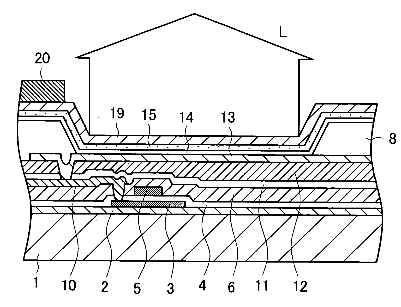
[0044]FIG. 1 is a sectional view of a top emission type organic electroluminescent display device according to the invention. In FIG. 1, a base film 2 for blocking impurities from glass is formed on a glass substrate 1. While there is a case in which one layer of a silicon nitride film or the like is formed as the base film 2, there is also a case in which the base film 2 is made of two layers, one each of a silicon nitride film and a silicon dioxide film. A semi-conductor layer 3 for configuring a TFT being formed on the base film 2, a gate insulating film 4 is formed covering the semi-conductor layer 3. In the embodiment, the semi-conductor layer 3 is an amorphous silicon film converted into a poly-silicon film by a laser annealing. A gate electrode 5, which is one portion of a gate wiring 5, is formed on the gate insulating film 4. The TFT of FIG. 1 is a top gate type TFT.

[0045]An inter-layer insulating film 6 being formed covering the gate electrode 5, a source / drain wiring (an ...

second embodiment

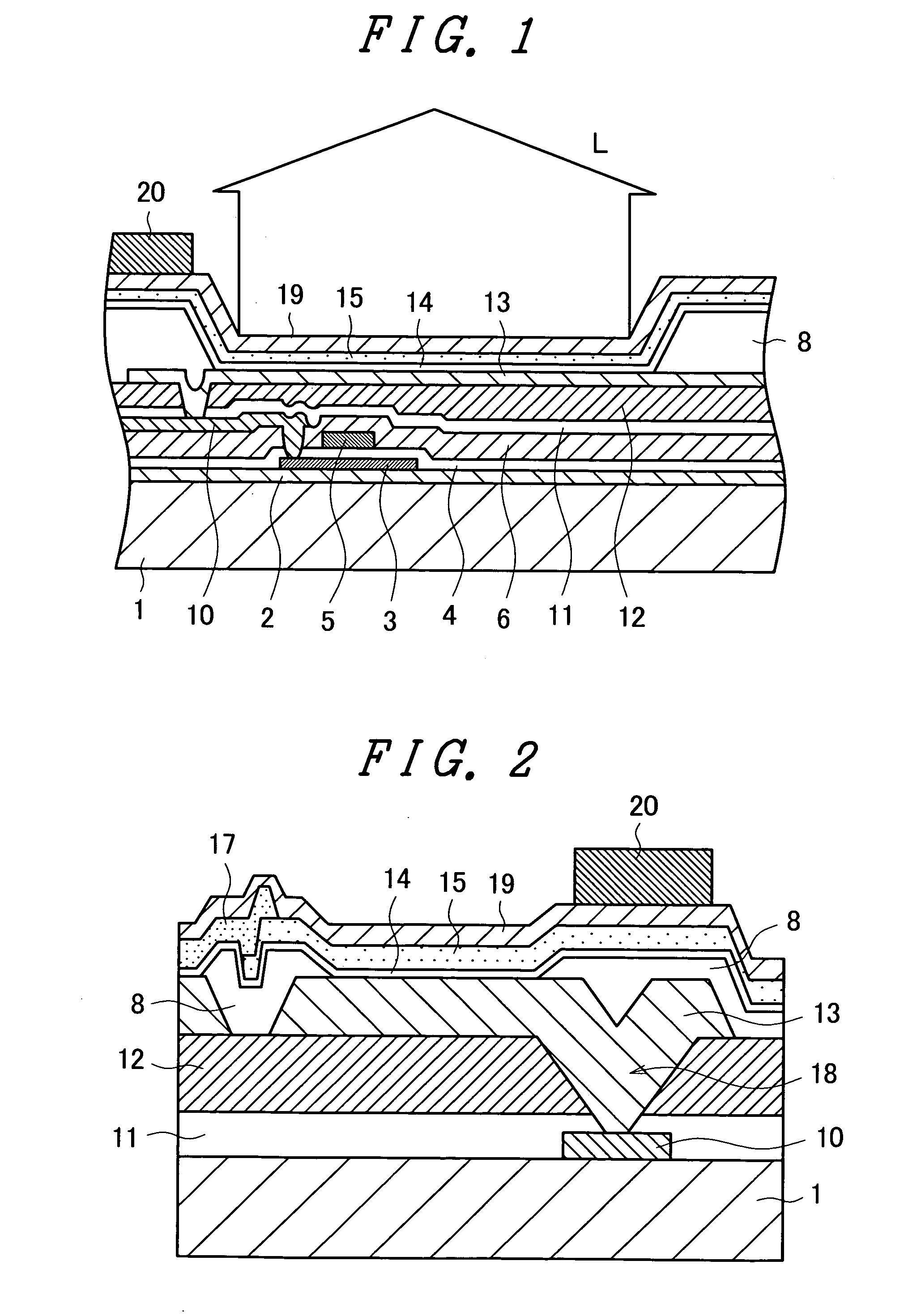
[0067]FIG. 4 is a sectional view of a second embodiment of the invention. A difference between the embodiment and the first embodiment lies in a point that the bank 8 is not formed between the lower electrodes 13. By forming the bank 8, the number of processes increases, as it is necessary to pattern a photosensitive acryl resin by means of a photolithography. Also, an acryl resin etching residue remains on the lower electrode 13, and this has an adverse effect on a light emitting property of the organic electroluminescent layer.

[0068]Although, in order to eliminate this kind of problem, the embodiment has a configuration which does not need the bank 8, even with this kind of configuration, it is possible to apply the configuration of the invention which does not carry out a patterning on the transparent conduction film 14 on the lower electrode 13. In FIG. 4, up to the formation of the planarizing film 12 is the same as the first embodiment shown in FIG. 1.

[0069]The lower electrode...

third embodiment

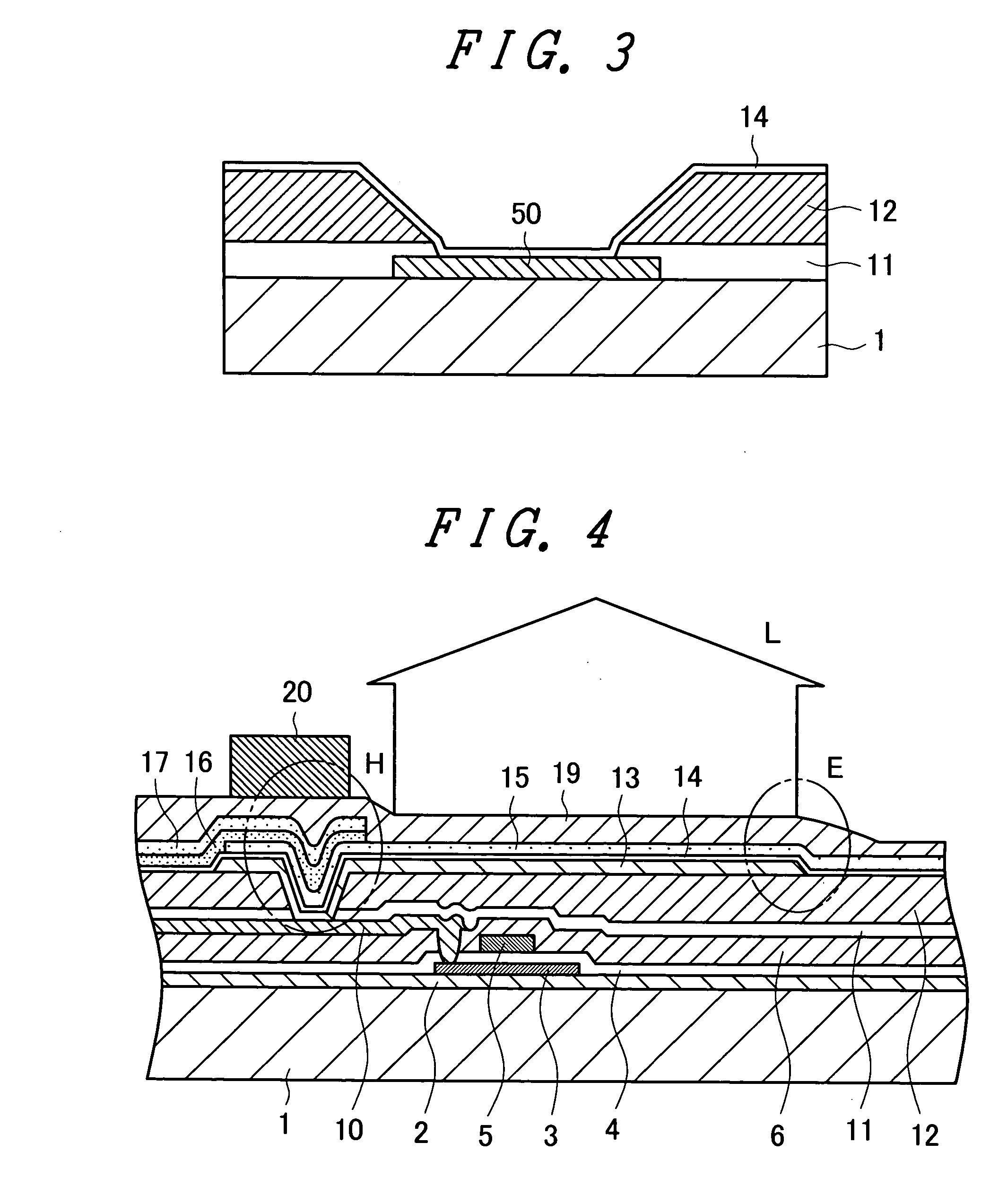
[0091]FIG. 11 is a sectional view of a pixel portion of a third embodiment of the invention. As with the second embodiment, the present embodiment does not form the bank 8 either. What the present embodiment differs from the second embodiment is the lower electrode 13, and a surface coating 131 of the lower electrode 13. In FIG. 11, up to the formation of the planarizing film 12 is the same as the first embodiment or the second embodiment. In the embodiment, as the bank 8 is not formed, the forming of a taper of 40 degrees or less at the extremity of the lower electrode 13, and forming a plurality of organic electroluminescent layers so as to overlap each other in the contact hole 18 are the same as in the second embodiment.

[0092]In the present embodiment, an aluminum-silicon alloy is used for the lower electrode 13. This is because an aluminum-silicon alloy has a high reflectivity, and generates only a small amount of dry etching residue. The aluminum-silicon alloy is deposited, by...


PUM


Abstract

To realize a top emission type organic electroluminescent display device which requires a small number of processes, and provides good color purity, and manufacturing yield. A transparent conduction film of 5 nm to 20 nm is formed on a lower electrode. An organic electroluminescent layer is sandwiched between the transparent conduction film and an upper electrode. The transparent conduction film is formed of indium tin oxide, and an indium tin oxide resistivity is controlled to a value of 1 to 105Ω·cm by controlling sputtering conditions. The electrical resistance of the indium tin oxide film controlled in this way can be low enough in a film thickness direction to supply a voltage to the organic electroluminescent layer, and, in a film planar direction, as high as in an insulated condition. Consequently, it is possible to maintain necessary properties even though the indium tin oxide is deposited over a whole of a substrate. According to the invention, it is possible to eliminate a process of patterning the indium tin oxide on the lower electrode.

Description

CLAIM OF PRIORITY[0001]The present application claims priority from Japanese Application JP 2007-229895 filed on Sep. 5, 2007, the content of which is hereby incorporated by reference into this application.BACKGROUND OF THE INVENTION[0002]1. Technical Field[0003]The present invention relates to a display device, particular relates to a top emission type organic electroluminescent display device which enables a lowering of a cost while maintaining a high image quality.[0004]2. Related Art[0005]As an organic electroluminescent display device, there are of a bottom emission type, which extracts a light emitted from an organic electroluminescent layer in a direction of a glass substrate on which are formed the organic electroluminescent layer and so on, and of a top emission type, which extracts the light in a direction opposite to the glass substrate on which are formed the organic electroluminescent layer and so on. The top emission type has an advantage in that, as it is possible to ...

Claims


Application Information

Patent Timeline
Patent Type & Authority Applications(United States)
IPC IPC(8): H01J1/62
CPCH01L27/3246H01L2251/5315H01L51/5234H01L51/5206H10K59/122H10K2102/3026H10K59/80518H10K59/80524H10K50/818H10K50/828
Inventor TANAKA, MASAHIROMATSUURA, TOSHIYUKI
Owner HITACHI DISPLAYS
Features
  • Generate Ideas
  • Intellectual Property
  • Life Sciences
  • Materials
  • Tech Scout
  • Unparalleled Data Quality
  • Higher Quality Content
  • 60% Fewer Hallucinations
Learn More