Nanostructure production methods and apparatus

a technology of nanostructures and production methods, applied in the field of nanostructure production methods, can solve the problems of severe limitations affecting application development, and achieve the effect of reducing heating effects on the substrate and increasing the range of materials

Active Publication Date: 2009-03-05
SURREY NANOSYST
View PDF13 Cites 16 Cited by
  • Summary
  • Abstract
  • Description
  • Claims
  • Application Information

AI Technical Summary

Benefits of technology

[0012]Viewed from a first aspect, the present invention relates to a method of forming nanostructures or nanomaterials comprising providing a thermal control barrier on a substrate and forming the nanostructures or nanomaterials. The thermal control barrier helps to ensure that the temperature of the substrate remains at a relatively low temperature and thereby increases the range of materials which may be used to form the substrate. Thus, the thermal control barrier reduces heating effects on the substrate. The temperature of the substrate is preferably less than 350° C. while the nanostructures or nanomaterials are formed.
[0013]At least in preferred embodiments of the present invention, it is now possible to deposit nanostructures or nanomaterials onto substrates at low temperatures while maintaining low defect levels, providing an increase in the commercial potential of carbon nanotube production, especially where nanostructures or nanomaterials are applied to commercially significant materials that could not be used with the known high temperature methods of deposition. The invention may also allow a higher yield and throughput in the synthesis of NSs due to increased growth rates.
[0022]The cooling of the substrate could be initiated immediately the nanostructures or nanomaterials have been formed. Preferably, however, the cooling of the substrate is performed while the nanostructures or nanomaterials are formed. Thus, the thermal control barrier can maintain the substrate at a relatively low temperature whilst allowing the nanostructures or nanomaterials to form.
[0033]The cooling of the second surface of the substrate is preferably performed uniformly over the whole of said surface. This helps to ensure uniform formation of the nanostructures or nanomaterials.
[0046]According to preferred embodiments of the present invention, there is provided a method of forming carbon nanotubes by plasma enhanced chemical vapour deposition using a carbon containing gas plasma, wherein the carbon nanotubes are not formed on a substrate at a temperature 350° C. or above. The carbon containing gas may be decomposed ex-situ of the growth environment, but enters the growth region in an excited or ‘hot plasma’ state such that it facilitates the growth process. The Carbon source would also be in the form of a plasma beam, or plasma arc, or molecular vapour with excited carbon ions or radicals. Obviously, with this invention, where the control over both heat to selective areas and material structure is attainable, could be extended to a host of other materials and applications.

Problems solved by technology

Current techniques involve substantial substrate temperatures and this imposes severe limitations on application development.

Method used


Image

  • Nanostructure production methods and apparatus
  • Nanostructure production methods and apparatus
  • Nanostructure production methods and apparatus

Examples


first embodiment

Description of First Embodiment

[0066]In this embodiment, the invention allows the deposition of low defect level carbon nanotubes, though not specifically, at low substrate temperature below 350° C. It should be clear to a skilled person that the invention can be extended to other materials.

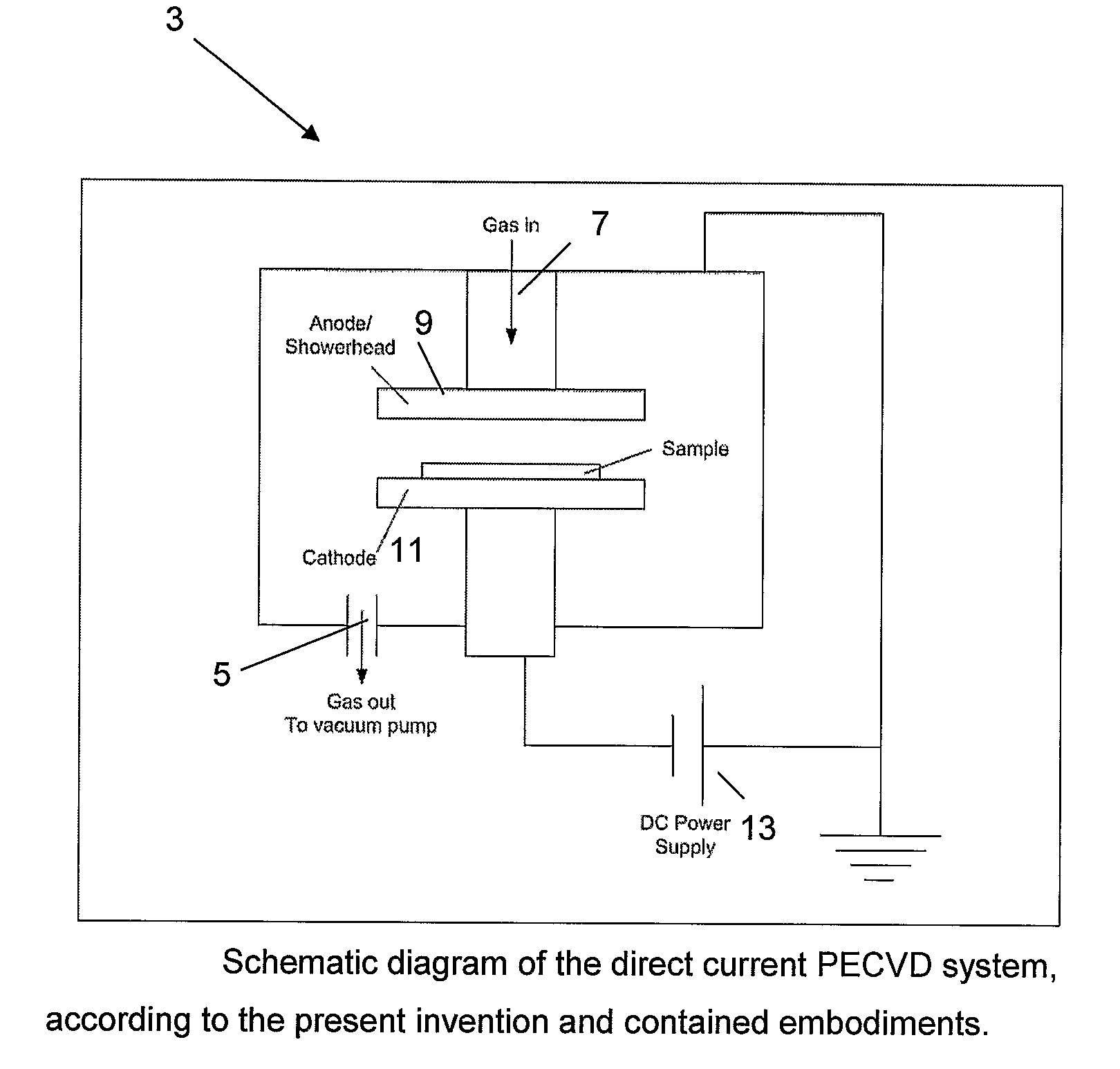
[0067]Referring firstly to FIG. 1, the plasma chamber 1 of a home built direct current PECVD system 3 is used as shown. A vacuum chamber housing is capable of evacuation with the pressure being controlled by a manual leak valve (not shown) at the vacuum pump inlet 5. The chamber has a gas inlet 7 for receiving a flow of the required gas or gaseous mixture, typically a hydrocarbon gas such as acetylene, C2H2. It should be obvious to a skilled person that any carbon containing gas could be used.

[0068]An earthed electrode (anode) 9 is also part of the shower head is provided in the upper part of the chamber 1, whilst a powered (negatively biased) electrode (cathode) 11 is provided in the lower part ...

second embodiment

Description of Second Embodiment

[0080]The invention according to the second embodiment allows the deposition of low defect level carbon nanotubes at low substrate temperature below 350° C. in the application of interconnects 27 used in microelectronics. Interconnects are used in integrated circuits for carrying large current densities. A suitable material would be the carbon nanotubes due to its covalent structure not subscribing to much electromigration, high current carrying capacity and ballistic electron transport capabilities giving rise to low resistivities for high current flows. Microelectronic processes often require substrate temperatures to be kept below 450° C. to prevent excessive diffusion of dopants through the increased creation of vacancies in silicon.

[0081]FIG. 6 shows the use of low thermal conductivity materials to isolate the heating from the neighbouring devices 29 such as transistors, etc. The location of the interconnect 27 can be defined through existing lit...

third embodiment

Description of Third Embodiment

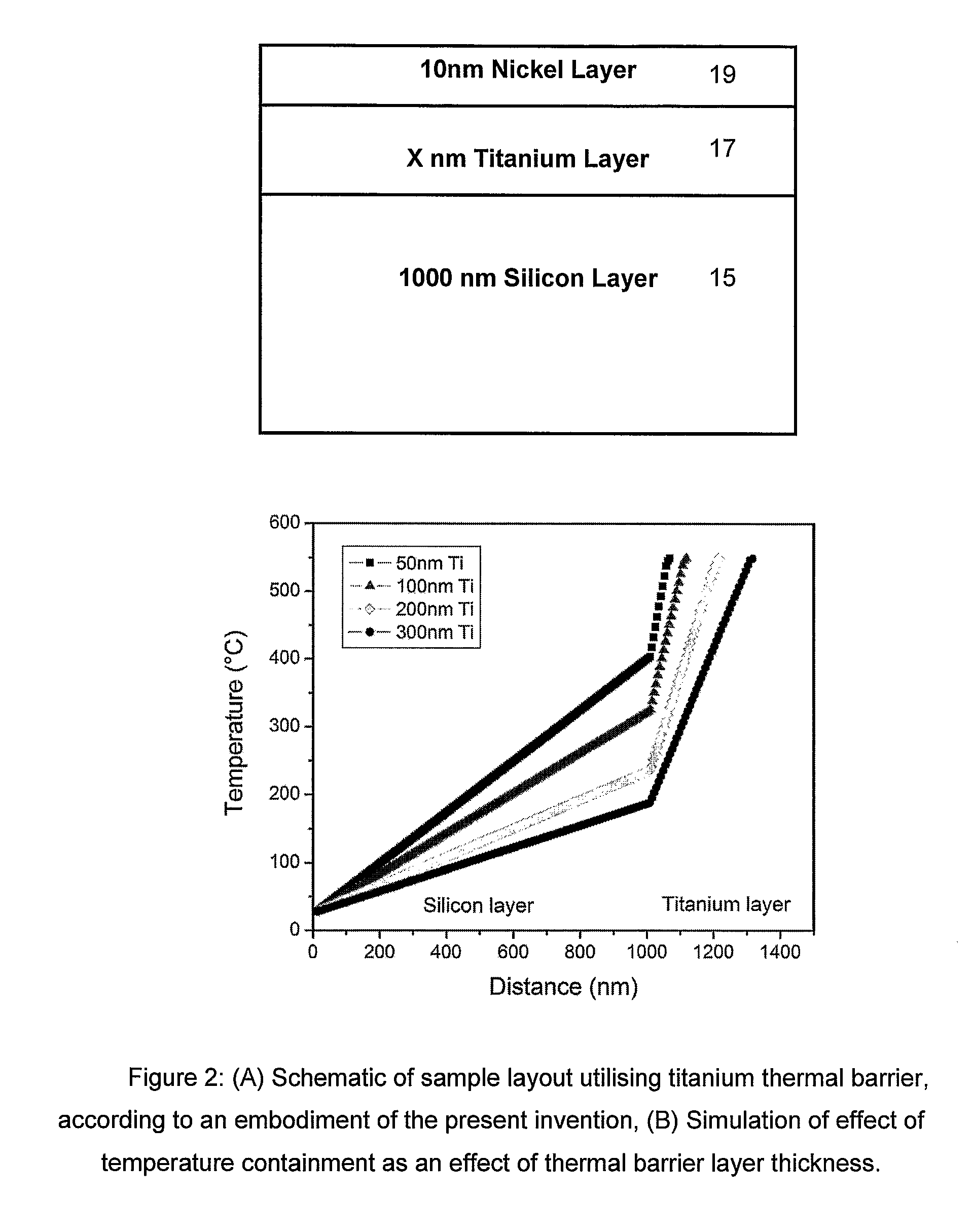
[0085]The invention according to the third embodiment allows the deposition of carbon nanotubes or alternative nanowires in a layer 28 at low substrate temperature below 350° C. in the application of sensing platforms. Carbon nanotubes or other nanowires are utilised as materials for chemical, mechanical, etc sensors due to their unique properties and high aspect ratio (which results in increased surface area). In this embodiment, a temperature sensitive substrate 15 such as plastic is used. A plurality of devices 29 are provided on the substrate 15. The use of temperature sensitive materials is not limited to substrates and can be extended to active devices such as organic transistors used in the application.

[0086]Referring to FIG. 7, the thermal barrier layer 17 can be described as enclosing the device region. The catalyst is laid on the required region and NTs are deposited using a similar technique as the first embodiment. A contact layer 18 is pro...


PUM

PropertyMeasurementUnit
temperatureaaaaaaaaaa
thicknessaaaaaaaaaa
temperaturesaaaaaaaaaa

Abstract

The present invention relates to a method of forming nanostructures or nanomaterials. The method comprises providing a thermal control barrier on a substrate and forming the nanostructures or nanomaterials. The method may, for example, be used to form carbon nanotubes by plasma enhanced chemical vapour deposition using a carbon containing gas plasma: The temperature of the substrate may be maintained at less than 350° C. while the carbon nanotubes are formed.

Description

FIELD OF THE INVENTION[0001]This invention relates to a method of making nanostructures at low substrate temperatures. More specifically, the invention concerns a method which uses a thermal control barrier and, optionally, a heating source that heats the surface of the targeted substrate.[0002]The term ‘nanostructures’ (NSs) is used herein as a generic term to embrace all metallic, semiconducting and insulating nanostructures which have high aspect ratio such as single-walled and multi-walled carbon nanotubes, carbon nanofibres, carbon nanofilaments, carbon nanoropes (ropes of carbon nanotubes), silicon and silicon oxide nanowire, gallium nitride nanowires, zinc oxide nanowire, etc. The term heat source is used herein as a generic term to represent all forms of heating such as resistive, optical, plasma, etc based.BACKGROUND TO THE INVENTION[0003]Nanostructures with high aspect ratios have great potential in a great variety of applications. Their small size resulting in quantum con...

Claims


Application Information

Patent Timeline
Patent Type & Authority Applications(United States)
IPC IPC(8): B32B9/00B05D3/10B05D3/06B32B5/00B05D5/12C23C16/513C01B31/02C23C16/46
CPCB82Y30/00B82Y40/00Y10T428/265C23C16/46C01B31/0233C01B32/162C23C16/26B82B3/00
Inventor SILVA, SEMBUKUTIARACHILAGE RAVIJENSEN, BEN PAULCHEN, GUAN YOW
Owner SURREY NANOSYST
Why Eureka
Try Eureka