

Method to create high efficiency, low cost polysilicon or microcrystalline solar cell on flexible substrates using multilayer high speed inkjet printing and, rapid annealing and light trapping
a solar cell, high-speed technology, applied in the direction of sustainable manufacturing/processing, final product manufacturing, coatings, etc., can solve the problems of high silicon price, low fundamental cost of manufacturing, and high cost of silicon processing, so as to achieve rapid laser annealing and low manufacturing cost , the effect of high efficiency
- Summary
- Abstract
- Description
- Claims
- Application Information
AI Technical Summary
Benefits of technology
Problems solved by technology
Method used
Image

Examples
first embodiment
[0100]Superstrate
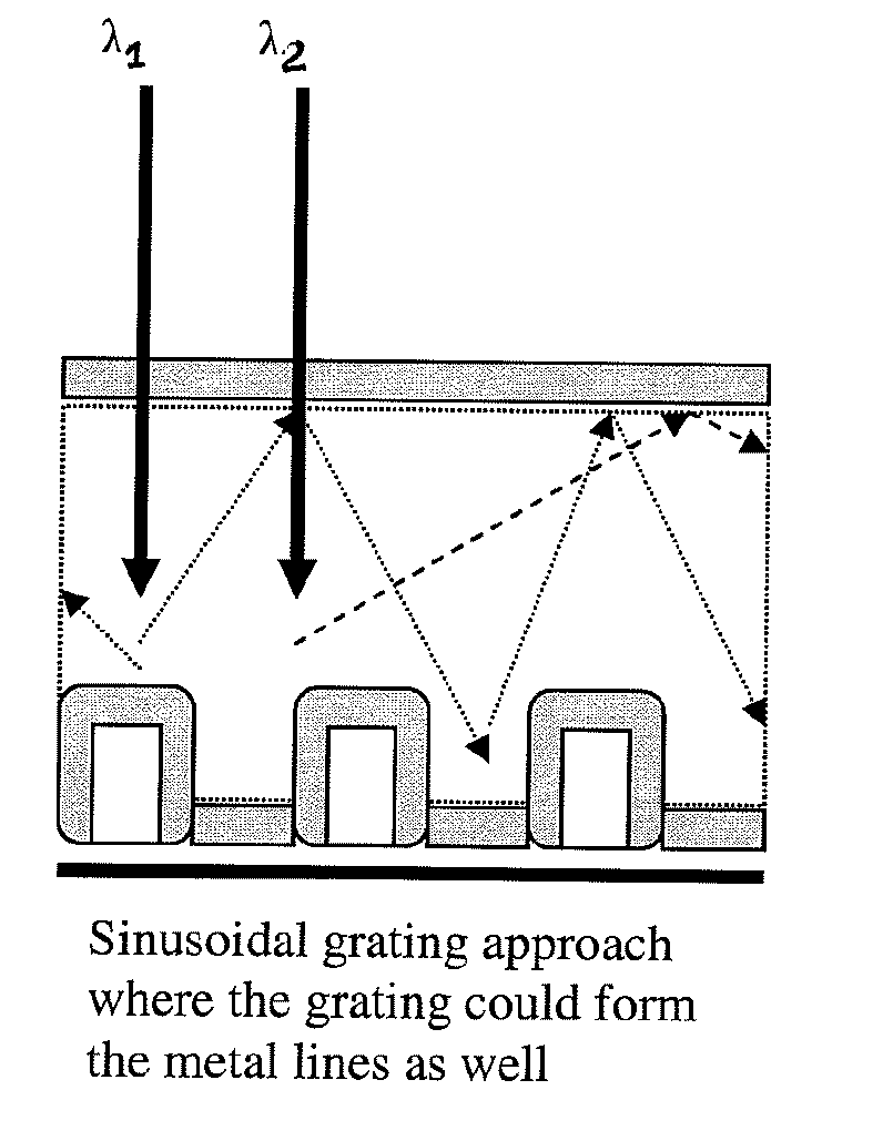
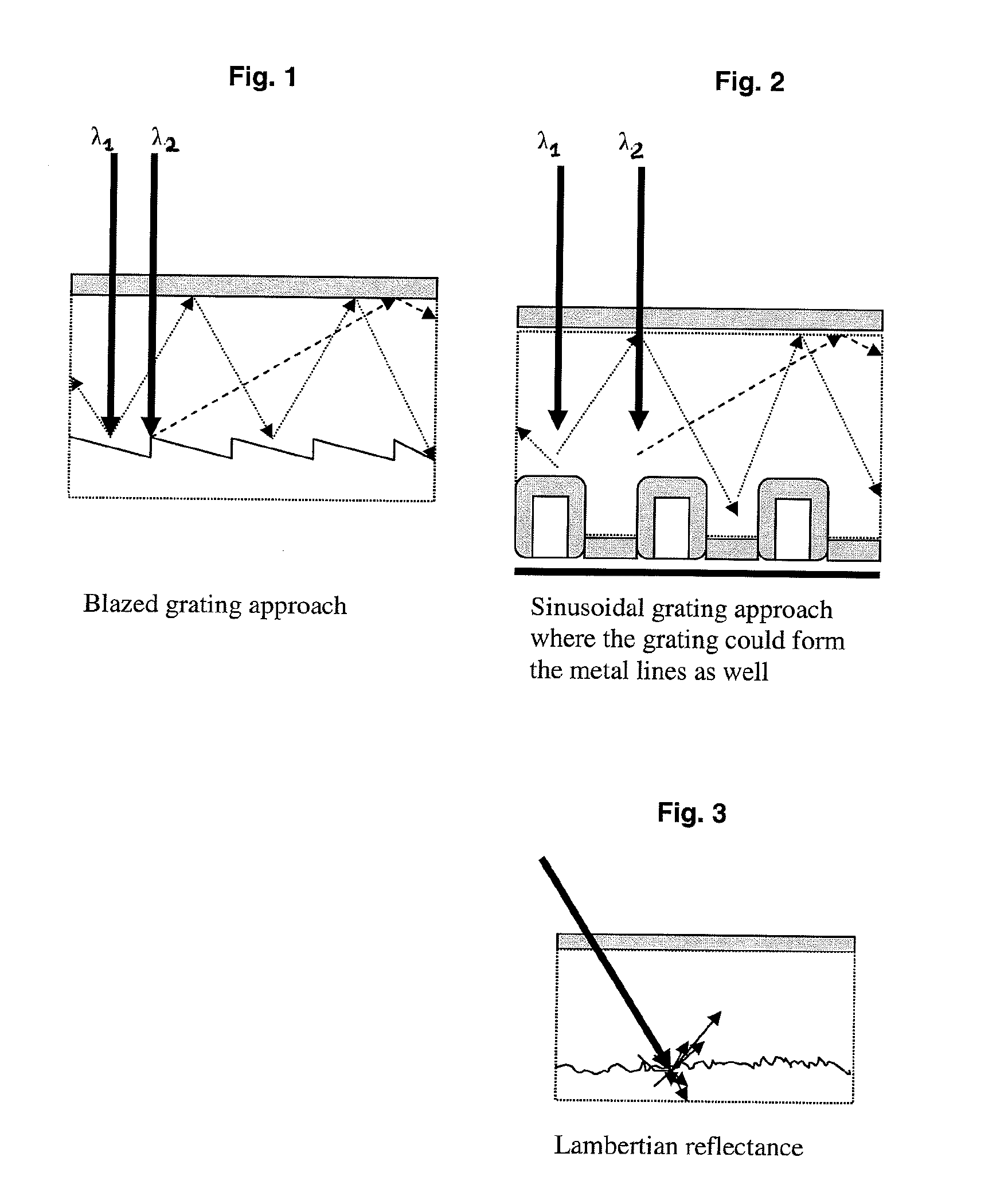
(1) Clean the flexible substrate and etch to texture the surface. Gratings can also be patterned on the flexible substrate.
(2) Inkjet print an adhesion promoter film
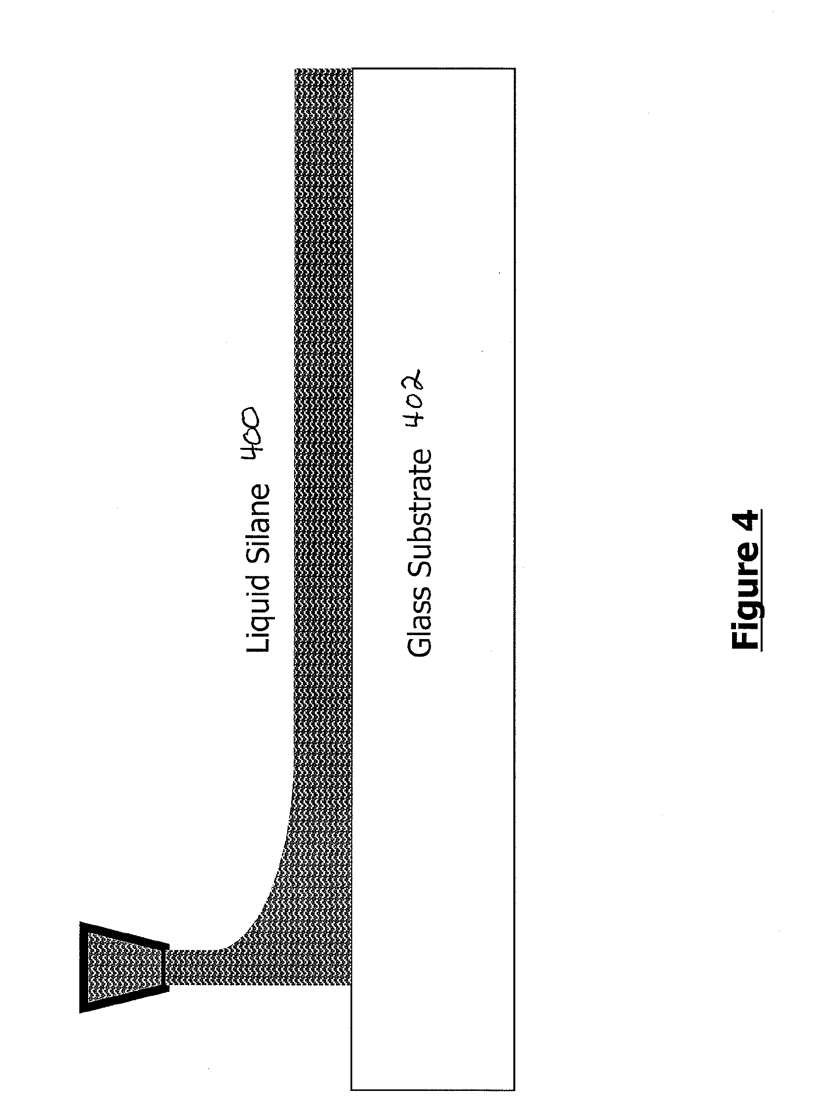
(3) Inkjet print p-type amorphous silicon
(4) Inkjet print p-type amorphous silicon. For undoped amorphous silicon films, an additional process step requiring spin-on dopant films will be needed.
(5) The amorphous silicon film will be annealed using laser or RTA to crystallize the films and reduce defects. Both the inkjet printing of the absorber and the annealing can be done in a nitrogenous atmosphere.
(6) A transparent conductive oxide layer will then be inkjet printed followed by inkjet printing of an antireflective coating.
(7) Spin coat or inkjet print the encapsulant
(8) Laser scribing will be used to isolate the cells and to create the contacts.
(9) The contact metallization will then be inkjet printed to create the functional solar cells.
second embodiment
[0101]Superstrate
(1) Clean flexible or fixed substrate. In some embodiments, etch to texture surface or pattern grating structures on the surface.
(2) Deposit Transparent Conductive Oxide. If deposited by CVD or coated as a liquid paste, the film can be automatically textured during deposition. If the film is formed by sputtering, an acid or plasma treatment textures the film after deposition,
(3) Using a laser, burn (cut) isolation lines in the TCO layer in order to isolate the individual photovoltaic cells. Clean substrate.
(4) Optionally, coat an adhesion promoter film.
(5) Coat a p-type amorphous silicon.
(6) Coat an n-type amorphous silicon. For undoped amorphous silicon films, an additional process step requiring spin-on dopant films may be needed. Alternatively, rather than coating with an n type material, the film can be doped using a diffusion furnace or optical annealing system in a POCl3 or other atmosphere.
(7) The amorphous silicon film is annealed using a laser to crystalliz...
embodiment
[0102]Substrate
(1) Clean flexible or fixed substrate. In one embodiment, etch to texture surface or pattern grating structures on the surface.
(2) Coat or vacuum deposit aluminum or other metal layer. If coated, the substrate would be fired to remove liquid to form solid coating. Etch if needed to texture film. Optionally, deposit second thin metal layer to block aluminum from dissolving in silicon to form eutectic.
(3) Using a laser, burn (cut) isolation lines in the metal layers in order to isolate the individual photovoltaic cells. Clean substrate.
(4) Optionally, coat an adhesion promoter film.
(5) Coat p-type amorphous silicon.
(6) Coat n-type amorphous silicon. For undoped amorphous silicon films, an additional process step requiring spin-on dopant films will be needed. Alternatively, rather than coating with an n type material, the film can be doped using a diffusion furnace or optical annealing system in a POCl3 or other atmosphere.
(7) Anneal the amorphous silicon film using lase...
PUM
| Property | Measurement | Unit |
|---|---|---|
| grain size | aaaaa | aaaaa |
| thickness | aaaaa | aaaaa |
| grain sizes | aaaaa | aaaaa |
Abstract
Description
Claims
Application Information