Self-segregating multilayer imaging stack with built-in antireflective properties

a multi-layer imaging and self-segregation technology, applied in the field of deep ultraviolet (duv) photolithography and semiconductor fabrication, can solve the problems of increased cost, increased cost of ownership, and more complex integration path, and achieve the effect of reducing the number of processing steps

Inactive Publication Date: 2010-01-14
GLOBALFOUNDRIES INC
View PDF19 Cites 23 Cited by
  • Summary
  • Abstract
  • Description
  • Claims
  • Application Information

AI Technical Summary

Benefits of technology

[0022]The self-segregating nature of the materials and formulation described in the present invention reduces the number of processing steps that are required to form a multilayer imaging stack, as well as the volume of ch

Problems solved by technology

Such approach encompasses doubling the number of all photomasks used for “double exposure'” as well as doubling processing time, tool time and materials usage, resulting in increased cost.
If adopted, this particular technology solution is expected to be applied to multiple levels resulting in a significant increase in cost of ownership (COO).
One of the disadvantages of using a trilayer stack is the longer processing time and increased number of processing steps, which results in a more complex integration path.
Reflection of light from the substrate/resist interface produces variations in the light intensity and scattering in the resist during exposure, resulting in non-uniform photoresist line width upon development.
Light can scatter from the interface into regions of the resist where exposure was not intended, resulting in line width variations.
The amount of scattering and reflection will typically vary from region to region resulting in line width non-uniformity.
Unfortunately, due to resist/substrate interface reflections, constructive and destructive interference is particularly significant when monochromatic

Method used


Image

  • Self-segregating multilayer imaging stack with built-in antireflective properties
  • Self-segregating multilayer imaging stack with built-in antireflective properties
  • Self-segregating multilayer imaging stack with built-in antireflective properties

Examples


examples

[0054]Examples 1 and 2 show two embodiments of this invention for lithographic applications and illustrate the properties and advantages of the materials and formulations described.

example 1

[0055]A formulation was prepared by dissolving 402 mg of resist polymer (50:50 copolymer of 1,1,1-trifluoro-2-trifluoromethyl-2-hydroxy-pent-4-yl methacrylate and 1-ethylcyclopentyl methacrylate), 160 mg of solution of triphenylsulfonium nonaflate (20 wt % in PGMEA), 402 mg of silsesquioxane (SSQ) polymer (60:40 copolymer of 1-(4-acetoxyphenyl)ethyl-SSQ and 1-phenylethyl-SSQ) and 883 mg of solution of N-phenylbenzimidazole (0.5 wt% in PGMEA) in 5.67 g of PGMEA. The solution was filtered through 0.2 μm syringe filter.

example 2

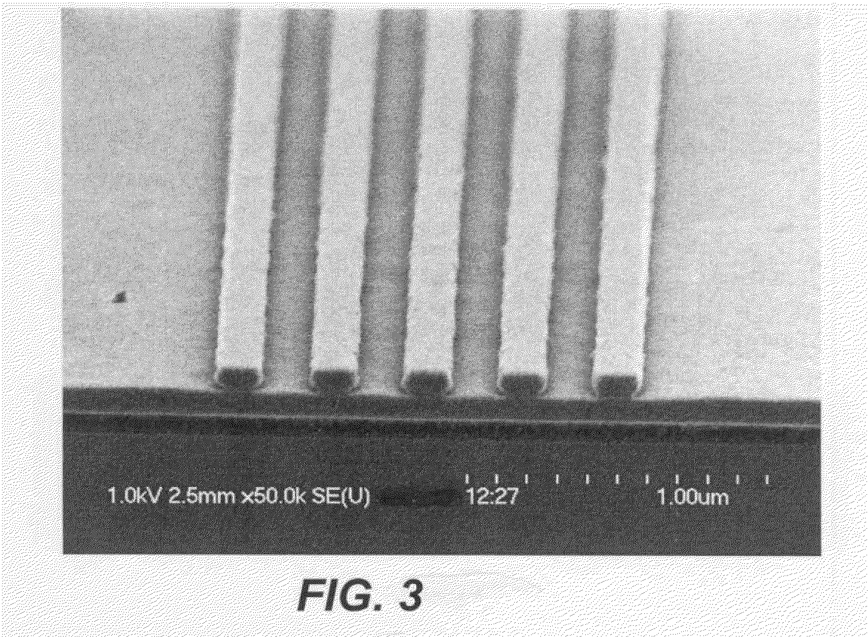
[0056]The formulation of EXAMPLE 1 was spin-coated at 3000 RPM on a wafer that was previously coated with ARC-29A (Brewer Sci. 78 nm) and baked at 155° C. for 90 seconds. The wafer was then exposed using a 193 nm ministepper (NA=0.6, binary mask) using 160 nm line-and space mask pattern. The wafer was then baked at 110° C. for 60 seconds and puddle-developed in a standard 0.26N N tetramethyl ammonium hydroxide (TMAH) developer for 30 seconds, rinsed with water, and dried. FIG. 3 illustrates the SEM cross-sections of patterns obtained.

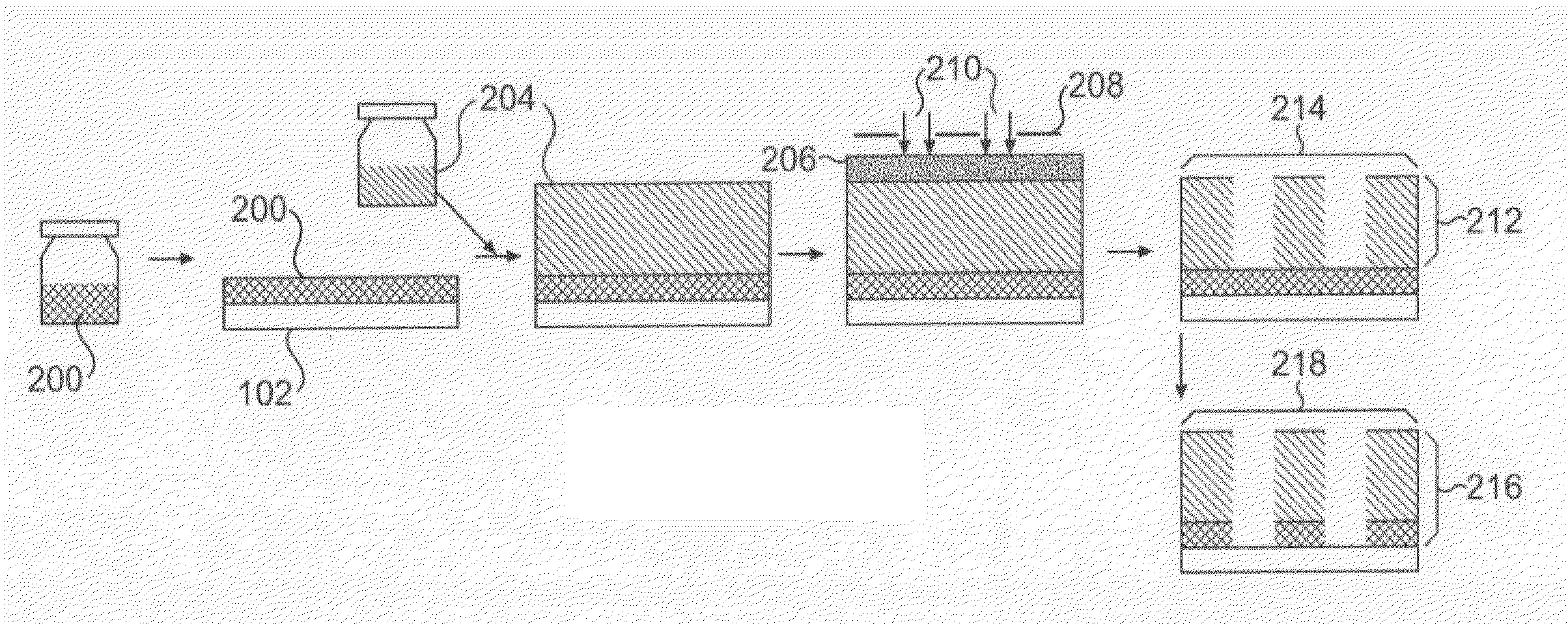
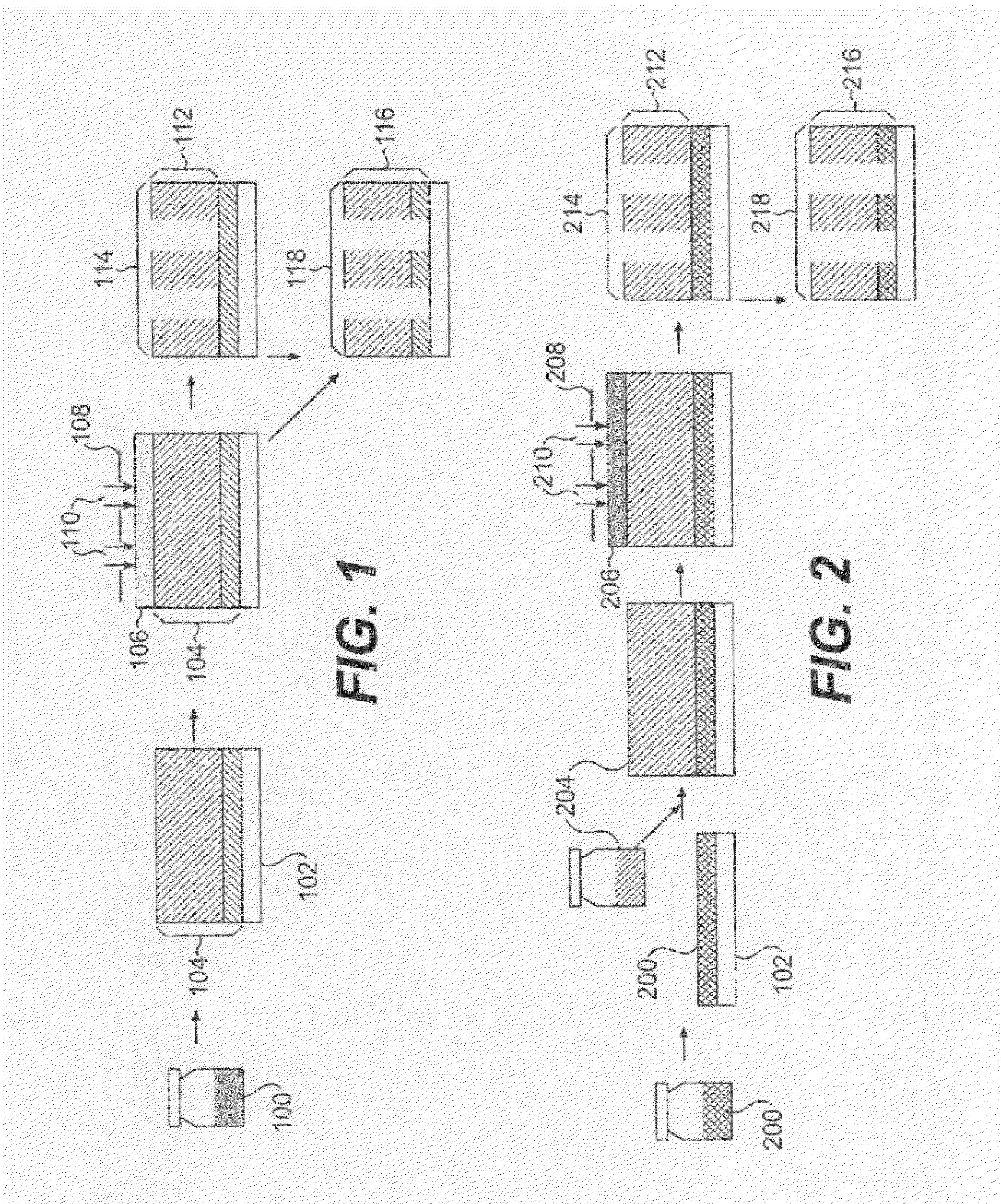
[0057]In use, FIG. 1 illustrates a processing sequence using a self-segregating Resist / BARC imaging system according to the present invention. In FIG. 1, a formulation 100 containing multiple components and additives for the formation of a self-segregated resist / BARC multilayer as described herein is spin-cast onto a wafer 102 and baked. The vertical segregation process takes place during the coating and / or baking step, leading to the formation of a res...


PUM

PropertyMeasurementUnit
Thicknessaaaaaaaaaa
Thicknessaaaaaaaaaa
Wavelengthaaaaaaaaaa

Abstract

A coating process comprises forming a patterned material layer on a substrate using a self-segregating polymeric composition comprising a polymeric photoresistive material and an antireflective coating material. The polymeric photoresistive material and the antireflective coating material that make up the self segregating composition are contained in a single solution. When depositing this solution on a substrate and removing the solvent, the two materials self-segregate into two layers. The substrate can comprise one of a ceramic, dielectric, metal, or semiconductor material and in some instances a material such as a BARC material that is not from the self segregating composition. The composition may also contain a radiation-sensitive acid generator and a base quencher. This produces a coated substrate having a uniaxial bilayer coating oriented in a direction orthogonal to the substrate with a top photoresistive coating layer and a bottom antireflective coating layer. The process may also include optionally coating a top coat material on the coated substrate. Pattern-wise exposing the coated substrate to imaging radiation and contacting the coated substrate with a developer, produces the patterned material layer wherein the optional top coat material and a portion of the photoresist layer are simultaneously removed from the coated substrate, thereby forming a patterned photoresist layer on the substrate. Alternatively, the optional top coat material, a portion of the photoresist layer and a portion of the bottom antireflective layers are simultaneously removed from the coated substrate by the developer, thereby forming a patterned photoresist layer on the substrate.

Description

FIELD OF THE INVENTION [0001]The present invention relates to the fields of deep ultraviolet (DUV) photolithography and semiconductor fabrication. More specifically, the invention relates to a processing scheme for a spin-castable, or spin-on, or spin-coating multi-component organic formulation with a reduced number of processing steps wherein the individual polymeric materials composing the formulation have the ability to vertically segregate during the coating and / or annealing steps to form a multilayer imaging stack.BACKGROUND OF THE INVENTION AND RELATED ART[0002]The constant demand for shrinking device sizes by the semiconductor industry requires continuous improvement in resolving power in state-of-the-art lithography tools. For example, immersion lithography has arisen as an effective enhancement technique to extend the resolution limits of optical lithography, and is expected to enable manufacturing of highly integrated circuits at the 45 nm node in 2008. Resolution requirem...

Claims


Application Information

Patent Timeline
IPC IPC(8): G03F7/20G03F7/004B32B3/10
CPCG03F7/0752G03F7/091Y10T428/24802Y10S438/952Y10S430/136
Inventor CHENG, JOYGOLDFARB, DARIO L.MEDEIROS, DAVID R.SANDERS, DANIEL P.PFEIFER, DIRKVYLICKY, LIBOR
Owner GLOBALFOUNDRIES INC
Why Eureka
Try Eureka