Method of producing semiconductor device using resist underlayer film by photo-crosslinking curing

a technology of resist and underlayer film, which is applied in the direction of photosensitive materials, instruments, photomechanical equipment, etc., can solve the problems of difficult application of organic materials, large influence of diffuse reflection of activating light rays from the substrate or the influence of standing waves, and low molecular mass, so as to enhance the homogeneity of the film thickness of a photoresist or the like applied and formed on the substrate, the effect of contamination of peripheral devices

Active Publication Date: 2010-01-28
NISSAN CHEM IND LTD
View PDF8 Cites 12 Cited by
  • Summary
  • Abstract
  • Description
  • Claims
  • Application Information

AI Technical Summary

Benefits of technology

[0030]According to the method of the present invention, by irradiating light, an excellent underlayer film having a dry etching rate larger than that of a photoresist and causing no intermixing with a photoresist can be formed.
[0031]In addition, with the resist underlayer film forming composition used in the present invention, the surface of a semiconductor substrate having holes which have an aspect ratio expressed by height / diameter of 1 or more can be planarized. Therefore, the homogeneity of the film thickness of a photoresist or the like applied and formed on the substrate can be enhanced. Then, even in a process using a substrate having holes, an advantageous photoresist pattern can be formed.
[0032]With the resist underlayer film forming composition used in the present invention, holes formed in a semiconductor substrate can be filled with an underlayer film without causing voids.
[0033]In addition, with the underlayer film forming composition used in the present invention, an underlayer film can be formed by irradiating light without heating at a high temperature. Therefore, the contamination of peripheral devices due to volatilization or sublimation of low molecular mass components contained in the underlayer film forming composition can be prevented. When the low molecular mass components are volatilized or sublimated, it is feared that the sublimated components are attached to the inside of a draft chamber and before long, these components fall onto a semiconductor substrate to cause a failure in a semiconductor. However, in the method according to the present invention, since heating at a high temperature is not necessary, even when low molecular mass components are used in a resist underlayer film forming composition, there is no fear of generating a sublimate or the like, so that a relatively large amount of low molecular mass components can be used in a resist underlayer film forming composition. Therefore, an underlayer film can be formed using a resist underlayer film forming composition having a relatively low viscosity. Then, a resist underlayer film excellent in filling property of holes and planarizing property of a semiconductor substrate can be formed.
[0034]The present invention is a method of producing a semiconductor device including: forming a coating film by applying a resist underlayer film forming composition containing a polymer, a crosslinker and a photoacid generator on a semiconductor substrate; forming an underlayer film by irradiating light to the coating film; forming a photoresist by applying a photoresist composition on the underlayer film and by heating the resultant coating film.
[0035]The resist underlayer film used in the present invention contains a polymer having a benzene ring, a hetero ring or a combination thereof in the main chain constituting the polymer or side chains bonded to the main chain. This polymer is preferably a polymer having a benzene ring, a hetero ring or a combination thereof in side chains bonded to the main chain constituting the polymer.

Problems solved by technology

Following such a tendency, the influence of diffuse reflection of an activating light ray from the substrate or the influence of a standing wave has become a large problem.
However, it is difficult to apply an organic material for a reflection preventing film to a substrate having a large aspect ratio and recently, materials focusing on the filling characteristics and the planarization characteristics have been developed (for example, see Patent Document 2, Patent Document 3, Patent Document 4 and Patent Document 5).
And now, these organic underlayer films are generally formed by applying an underlayer film forming composition on a semiconductor substrate and then by heating the semiconductor substrate at a high temperature of around 170 to 200° C. Therefore, there is such a problem that during heating at a high temperature, low molecular mass components contained in an underlayer film forming composition are volatilized or sublimated, and are attached to peripheral devices to contaminate the devices.
In addition, there is also such a problem that the components attached to the devices fall onto a semiconductor substrate to adversely affect a pattern forming.

Method used


Image

  • Method of producing semiconductor device using resist underlayer film by photo-crosslinking curing
  • Method of producing semiconductor device using resist underlayer film by photo-crosslinking curing
  • Method of producing semiconductor device using resist underlayer film by photo-crosslinking curing

Examples


synthesis example 1

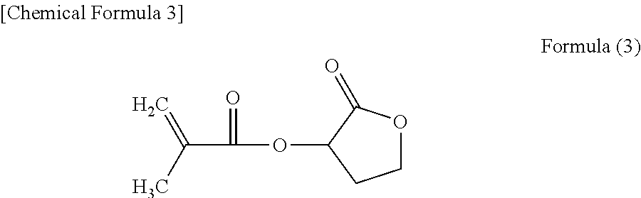
[0110]6.6 g (0.039 mol) of butylolactone methacrylate of Formula (3):

[0111]6.6 g (0.046 mol) of hydroxypropyl methacrylate and 6.8 g (0.039 mol) of benzyl methacrylate were dissolved in 64.4 g of tetrahydrofuran and then the inside of a flask was replaced by nitrogen, followed by elevating the temperature of the solution to a reflux temperature. After the start of the reflux, 0.2 g of azobis-isobutylonitrile (AIBN) dissolved in 10 g of tetrahydrofuran was added to the reaction solution under nitrogen pressure and the reaction was effected for 24 hours. The reaction solution was cooled and then charged into diethyl ether, and a polymer was reprecipitated therein. The obtained polymer was dried by heating and a resin of Formula (4) was obtained. The obtained resin had a polymerization degree of 490, a weight average molecular mass Mw of 80,000 (converted into the mass of polystyrene), a molar ratio x:y1:y2 of 31%:38%:31% and a yield of 90%.

example 1

[0112]To 8.0 g of an ethyl lactate solution (solid content concentration: 20.0%) containing 1.6 g of the resin obtained in Synthesis Example 1, 0.4 g of tetramethoxymethyl glycoluryl as a crosslinker and 0.03 g of triphenylsulfonium trifluoromethanesulfonate as a photoacid generator were blended. The resultant reaction mixture was dissolved in 55 g of propyleneglycol monomethyl ether acetate and 6.5 g of ethyl lactate which are reaction solvents to prepare a 10.0% solution. Thereafter, the solution was filtered, first by using a polyethylene-made microfilter having a pore diameter of 0.10 μm, and next by using a polyethylene-made microfilter having a pore diameter of 0.05 μm to prepare a resist underlayer film forming composition.


PUM

PropertyMeasurementUnit
temperatureaaaaaaaaaa
aspect ratioaaaaaaaaaa
temperatureaaaaaaaaaa

Abstract

There is provided a resist underlayer film forming composition used in a lithography process for producing semiconductor devices. A method of producing a semiconductor device comprising: forming a coating film by applying a resist underlayer film forming composition containing a polymer, a crosslinker and a photoacid generator on a semiconductor substrate; forming an underlayer film by irradiating light to the coating film; and forming a photoresist by applying a photoresist composition on the underlayer film and heating the resultant layer. The polymer polymer is a polymer having a benzene ring or a hetero ring in a main chain or a side chain bonded to the main chain, and the content rate of a benzene ring in the polymer is 30 to 70% by mass. The polymer may be a polymer containing a lactone structure.

Description

TECHNICAL FIELD[0001]The present invention relates to a method of forming an underlayer film between a semiconductor substrate and a photoresist by photo-crosslinking. In detail, the present invention relates to a method of producing a semiconductor device including: forming an underlayer film used as a photoresist underlayer in a lithography process for producing semiconductor devices by irradiating light. In addition, the present invention relates to a method of forming an underlayer film using the underlayer film forming composition and a method of forming a photoresist pattern.BACKGROUND ART[0002]Conventionally, in the production of a semiconductor device, fine processing by lithography using a photoresist has been performed. The fine processing is a processing method of forming fine convexoconcave corresponding to the following pattern on the surface of a substrate by forming a thin film of a photoresist on a semiconductor substrate, such as silicon wafer; irradiating an activa...

Claims


Application Information

Patent Timeline
Patent Type & Authority Applications(United States)
IPC IPC(8): H01L21/308
CPCG03F7/09Y10S430/114Y10S430/128G03F7/091G03F7/11H01L21/0276
Inventor HORIGUCHI, YUSUKETAKEI, SATOSHISHINJO, TETSUYA
Owner NISSAN CHEM IND LTD
Why Eureka
Try Eureka