Thin film capacitors on metal foils and methods of manufacturing same

a technology metal foils, applied in the field of thin film capacitors on metal foils, can solve the problems of low insulation resistance in barium titanate based compositions, inability to replace like conventional surface mounted capacitors, and troublesome achieving 100% embedded capacitor yield

Inactive Publication Date: 2010-03-25
CHEMTRON RES
View PDF10 Cites 14 Cited by
  • Summary
  • Abstract
  • Description
  • Claims
  • Application Information

AI Technical Summary

Problems solved by technology

Once the capacitors are embedded, however, they cannot be replaced like conventional surface mounted capacitors.
Achieving 100% embedded capacitor yield is especially troublesome where it is desirable for a large number of embedded capacitors to occupy the area under or proximate a semiconductor such as an IC mounted on the PWB.
The low oxygen partial pressures, however, often result in low insulation resistance in barium titanate based compositions due to reduction of the dielectric material.
Thus, larger area capacitors have lower insulation resistance.
However, the fabrication of large area CSD thin-film capacitors on metal foil has been limited by the defect density in the dielectric thin-film caused, for example, by the presence of cracks, porosity, voids, and pinholes.
Defects in the dielectric may form as a result of a variety of reasons, such as, for example, the effect of the underlying metal foil, dust particles in the fabrication area, inadequate densification of the dielectric, and defects or vacancies in the molecular structure.
This and the high level of refractoriness exhibited by high dielectric constant materials, makes achieving functioning large area capacitors wholly derived from CSD processing difficult.

Method used


Image

  • Thin film capacitors on metal foils and methods of manufacturing same
  • Thin film capacitors on metal foils and methods of manufacturing same
  • Thin film capacitors on metal foils and methods of manufacturing same

Examples


example 1

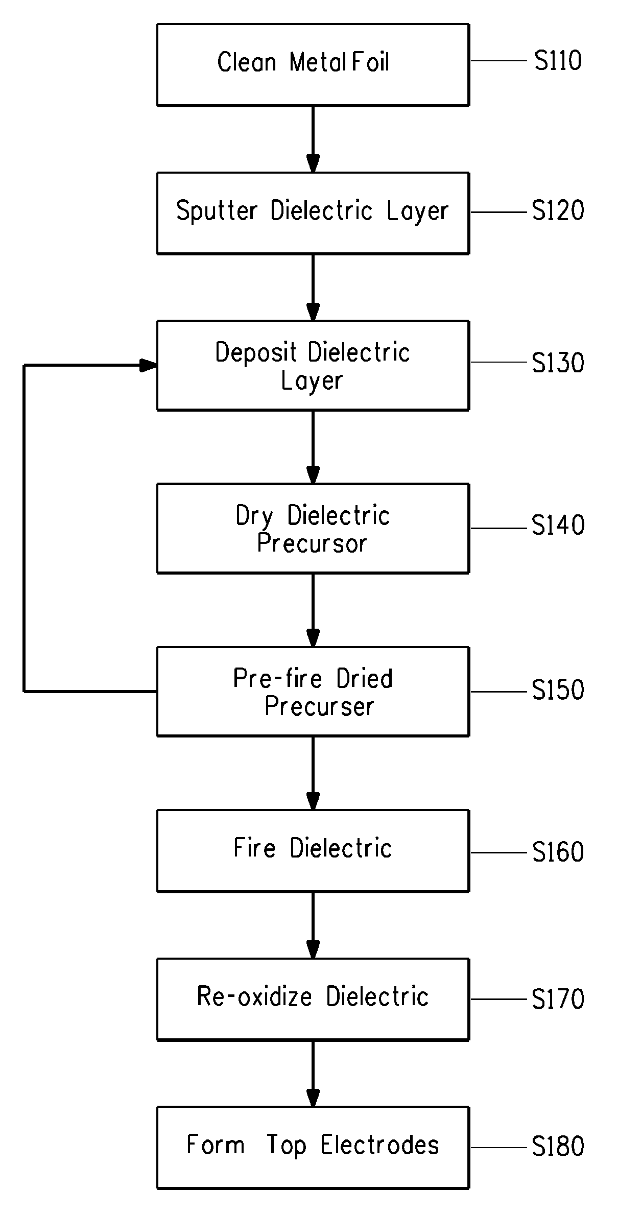
[0064]A barium strontium titanate (BST) first dielectric layer was sputtered on to the surface of nickel foil to a nominal thickness of 0.25 micrometer. The sputtering target was doped barium strontium titanate with a composition of Ba0.25Sr0.25Ti0.493528Mn0.0679Nb0.4Mg0.1793O3. The deposition was accomplished by radio frequency (RF) sputtering in argon using a deposition pressure of around 10 mtorr using an RF power of 200W. A nominal 0.4 mol (M) barium titanate dielectric precursor solution doped with a nominal 0.4 mole % manganese was spin-coated onto the sputtered BST first dielectric layer. The coating speed was 3000 rpm. The dielectric precursor solution was then dried in air for 7 minutes at 250° C. The dried dielectric precursor layer was then prefired for 10 minutes at 450° C. in a moist nitrogen / forming gas mixture that was created by bubbling a mixture of nitrogen and forming gas (99% nitrogen and 1% hydrogen) through a water bath at approximately 20° C. to create a gas a...

example 2

[0068]A barium strontium titanate first dielectric layer was sputtered on to the surface of nickel foil to a nominal thickness of 0.4 micrometers. The target composition and deposition conditions were as described in Example 1. A nominal 0.3 M barium titanate dielectric precursor solution doped with a nominal 0.4 mole % manganese was spin coated onto the sputtered BST first dielectric layer. The coating speed was 3000 rpm. The precursor solution was then dried in air for 7 minutes at 250° C. The dried precursor was then prefired for 20 minutes at 450° C. in air. The ramp rate of the furnace during the prefire heating phase was approximately 15° C. per minute. The same process of spin coating deposition, drying and prefiring at 450° C. in air was repeated 15 times to obtain the desired film thickness.

[0069]The multiple dried and prefired dielectric precursor layers, the sputtered BST first dielectric layer and the nickel foil were fired in a six inch internal diameter tube furnace at...

example 3

[0072]A barium strontium titanate first dielectric layer was sputtered on to the surface of nickel foil to a nominal thickness of 0.4 micrometers. The target composition and deposition conditions were as described in Example 1. The sputtered BST first dielectric layer and the Ni foil was then fired in a six inch internal diameter tube furnace at 900° C. for 20 minutes at peak temperature using the same ramp rate and furnace atmosphere conditions as described in Example 1. The partial pressure of oxygen at the firing temperature was approximately 10−15 atmospheres as measured by use of a zirconia cell placed inside the furnace. During the cooling process, the forming gas supply to the furnace was switched off at 600° C. so that the dielectric was exposed to pure nitrogen at a partial pressure of oxygen of approximately 10−6 atmospheres to reoxidize the dielectric without oxidizing the underlying nickel foil.

[0073]A nominal 0.3 M barium titanate dielectric precursor solution doped wit...


PUM

PropertyMeasurementUnit
temperatureaaaaaaaaaa
partial pressureaaaaaaaaaa

Abstract

Disclosed are methods of making a dielectric on a metal foil, and a method of making a large area capacitor that includes a dielectric on a metal foil. A first dielectric layer is formed over the metal foil by physical vapor deposition, and a dielectric precursor layer is formed over the first dielectric layer by chemical solution deposition. The metal foil, first dielectric layer and dielectric precursor layer are prefired at a prefiring temperature in the range of 350 to 650° C. The prefired dielectric precursor layer, the first dielectric layer and the base metal foil are subsequently fired at a firing temperature in the range of 700 to 1200° C.

Description

TECHNICAL FIELD[0001]The present invention pertains to capacitors that can be embedded in printed wiring boards, and more particularly to capacitors that include a thin film dielectric formed on a metal foil.RELATED ART[0002]A high capacitance density, thin-film ceramic capacitor can be embedded in a printed wiring board (PWB) package onto which an integrated circuit (IC) is mounted. A single layer ceramic capacitor directly under the IC can reduce the inductance and provide the capacitance necessary to satisfy the IC requirements. Such a capacitor in the PWB can provide capacitance at a significantly quicker response time and lower inductance than surface mounted capacitors.[0003]Embedment of high capacitance, ceramic thin-film capacitors in printed wiring boards is known. Capacitors are initially formed on metal foils by depositing a capacitor dielectric material on the foil and firing it at an elevated temperature. A top electrode is formed on the dielectric to form a fired-on-fo...

Claims


Application Information

Patent Timeline
Patent Type & Authority Applications(United States)
IPC IPC(8): H01G4/00B05D5/12
CPCH01G4/12H01G13/00H05K1/162H05K2201/0175H05K2201/0195H05K2201/0355Y10T29/49163Y10T29/435Y10T29/49155Y10T29/43Y10T29/49128Y10T29/49147H05K2203/1126
Inventor SUH, SEIGIKIM, ESTHERBORLAND, WILLIAM J.GROSS, CHRISTOPHER ALLENMACK, OMEGA N.OVERCASH, TIMOTHY R.
Owner CHEMTRON RES
Why Eureka
Try Eureka