

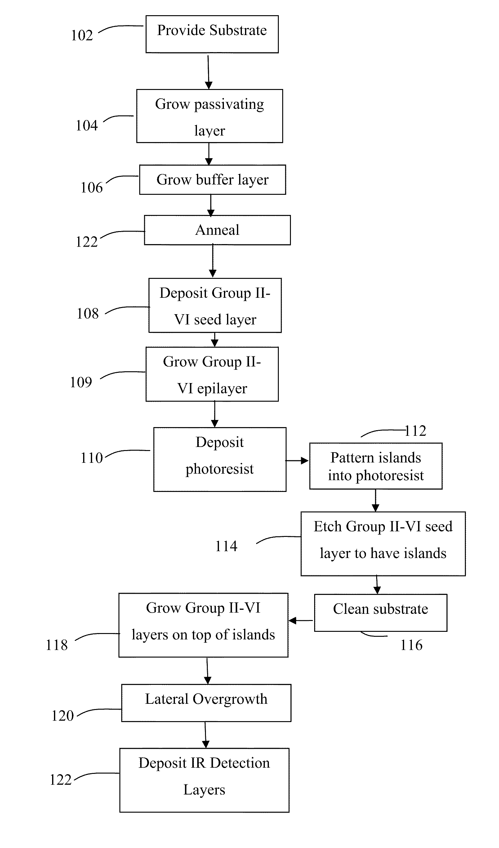
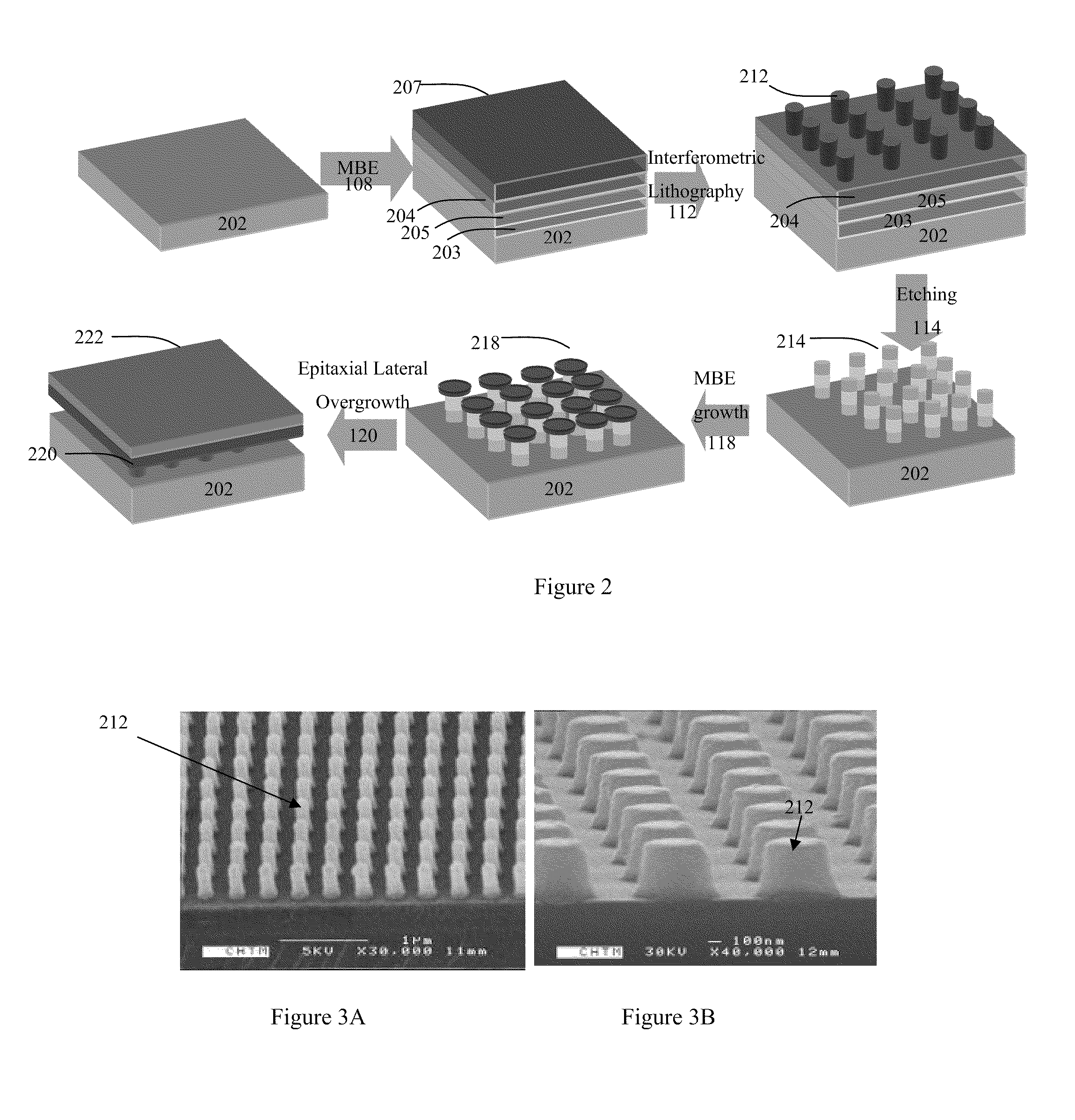
Nanostructures for dislocation blocking in group ii-vi semiconductor devices
a technology of nanostructures and semiconductor devices, applied in the field of nanostructures for dislocation blocking in group iivi semiconductor devices, can solve the problems of cdznte wafers, preventing the large scale commercialization of hgcdte-based infrared arrays, and severely constraining the size of cdznte substrates, so as to achieve the effect of increasing the durability of the semiconductor device and reducing the defect densities
- Summary
- Abstract
- Description
- Claims
- Application Information
AI Technical Summary
Benefits of technology
Problems solved by technology
Method used
Image

Examples
example 1
[0057]A 3-inch Si (211) wafer with approximately 5 μm CdTe grown by MBE was spun with photoresist SPR 1818 at 3000 rpm for 30 seconds and baked at 115° C. for 3 minutes. This wafer was then diced into 20 mm×20 mm pieces and the photoresist was stripped away in acetone (this photoresist layer was used to protect the CdTe epilayer from being damaged during the dicing of the wafer). The 20 mm×20 mm samples were then spun with a negative photoresist SU-8 @ 3000 rpm for 30 seconds and were subjected two different baking steps: 60 seconds @ 65° C. and 120 seconds @ 95° C. An iron oxide mask with a 320×256 array format having pixel regions of 5 μm on a 30 μm pitch was used on a MJB-3 mask aligner to perform contact lithography. The exposures were performed for 11 seconds and the samples were then baked in two steps: 60 seconds @ 65° C. and 120 seconds @ 95° C. These were then developed for 12 seconds in the SU-8 developer solution.
[0058]Optical microscope images of the photoresist are show...
example 2
[0075]SOI substrates 1400 (20 mm×20 mm pieces) were subjected to a chemical rinse in piranha and then deionized water. A layer 1402 of ARC (XHRI-16) was spun (step 1308) on the samples at 4000 rpm for 30 seconds and then hard baked at a temperature of 175° C. for 3 minutes. This process resulted in an ARC thickness of 150 to 160 nm. The bake allowed the ARC 1402 to sustain beam exposure without cracking The ARC 1402 was an organic polymer that serves to avoid standing wave patterns that would otherwise result from the interference between the incident laser beam and the reflected beam from the substrate.
[0076]The substrates were cooled for 60 seconds and then spun (step 1308) with a positive photoresist 1404 at 4000 rpm for 30 seconds. Subsequently, they were soft baked at 95° C. for 3 minutes. The SOI samples were exposed to ultraviolet (UV) radiation for 15 sec and then rotated by 90 degrees for a second exposure to obtain 2-D features. Following the UV exposure, the samples were ...
example 3
[0079]A custom holder suitable for holding 6 pieces of 10 mm×10 mm and 2 pieces of 20 mm×20 mm size was used for the CdTe growth on silicon nanopillars 1408. The samples were subjected to RCA cleaning and blown dry with nitrogen before being loaded into the introduction chamber and transferred into the preparation chamber, where they were prebaked at 500° C. for 8 hours. The samples were then transferred into the growth chamber under high vacuum and the temperature was ramped to 1050° C. The samples were left at that temperature for duration of 30 seconds to desorb the oxide on the silicon surface and subjected to an arsenic flux while ramping down the temperature to approximately 400° C. A CdTe nucleation layer 1410 was deposited for approximately two minutes at a temperature of between approximately 420° C. and approximately 470° C., preferably 440° C. The as-grown layer was then desorbed by ramping the temperature to between approximately 660° C. and 710° C., preferably 680° C., ...
PUM
 Abstract
Description
Claims
Application Information