Thin-film photoelectric conversion device

a conversion device and thin film technology, applied in the field of thin film photoelectric conversion devices, can solve the problems of insufficient refractive index difference, limited reflection properties of the entire multi-junction photoelectric conversion device, and insufficient satisfactory reflection properties, so as to improve the reflection properties of the front photoelectric conversion unit, improve the film quality and the transmission of the carbon layer, and improve the refractive index difference between the interlayer and the silicon layer.

Inactive Publication Date: 2010-09-30
KANEKA CORP
View PDF4 Cites 16 Cited by
  • Summary
  • Abstract
  • Description
  • Claims
  • Application Information

AI Technical Summary

Benefits of technology

[0049]According to the present invention, refractive index difference between an interlayer and a silicon layer is increased, and thus reflection properties to a front photoelectric conversion unit are improved. In addition, film quality and transmittance of the carbon layer are improved by a transparent oxide layer. Therefore, short-circuit current density is increased. Further, as compared with the case where only the carbon layer is inserted, a favorable interface bonding with the photoelectric conversion unit may be formed, so that series resistance is decreased to improve the properties.
[0050]Furthermore, as compared with the case where the carbon layer is formed into a film by one layer, stress resistance was remarkably improved by the stack of transparent oxide layer / carbon layer / transparent oxide layer / carbon layer / transparent oxide layer in this order. Thus, productivity was also improved. Adjusting film thickness of the transparent oxide layer and the carbon layer in the interlayer allows reflection properties to be steeply changed in an optional wavelength range of light. Thus, only light with a necessary wavelength for the front photoelectric conversion unit may be reflected by the interlayer so efficiently as to increase photoelectric conversion current.
[0051]Through the effects as described above, the present invention may provide a high-performance photoelectric conversion device.
[0052]Further, in the present invention, a hard carbon layer having electrical conductivity is inserted between a transparent electrode layer and a high reflecting electrode layer, so that the surface state of the transparent electrode layer is modified to form a favorable electrical contact with the high reflecting electrode layer. In addition, the high reflecting electrode layer having excellent reflection properties is formed to increase incident light into a generating layer. Absorption loss on an interface of a high reflecting electrode layer is decreased to bring the effect of increasing light scattering. According to the present invention, the hard carbon layer may be made of diamond-like carbon to improve conversion efficiency of a photoelectric conversion device by high transmittance and high electrical conductivity.

Problems solved by technology

The above-mentioned multi-junction structure allows incident light to be effectively utilized, however, the properties of the entire multi-junction photoelectric conversion device may be restricted.
However, considering that the refractive index of the conductive oxygenated silicon layer is approximately 1.95 and the refractive index of a silicon layer forming the photoelectric conversion units is approximately 3.3, satisfactory reflection properties are not obtained for the reason that a difference of refractive indexes is not sufficient.
However, a polycrystalline silicon layer is used as part of the multilayer film, in this case it is conceived that wavelength-selectivity is improved by refractive index differences in the multilayer film, but still sufficient reflection properties are not obtained by reason of being the same material and refractive index as a silicon layer forming the photoelectric conversion units.
Accordingly, the film thickness of the i-type layer as a photoelectric conversion layer is preferably thicker for light absorption, and thickening the i-type layer more than necessary increases cost and time for accumulation thereof.
However, these conductive layers are inactive layers and have no contribution to photoelectric conversion, and thus light absorbed by impurities doped into the conductive layers does not contribute to electric power generation but becomes loss.
However, the insertion of the transparent electrode layer is effective in the above-mentioned intention, but yet greatly influences the film quality of the high reflecting electrode layer depending on the forming conditions of the transparent electrode to cause functional depression as the reflecting layer.
Further, the transparent electrode layer occasionally becomes a barrier in electrical contact between the photoelectric conversion unit and the high reflecting electrode layer and does not sufficiently function as a take-out electrode, so that the properties as a solar cell are occasionally deteriorated.
In addition, absorption loss is caused in an interface between the transparent electrode layer and the high reflecting electrode layer to substantially decrease incident light into a silicon layer and decrease the properties of a solar cell.

Method used


Image

  • Thin-film photoelectric conversion device
  • Thin-film photoelectric conversion device
  • Thin-film photoelectric conversion device

Examples


example 1

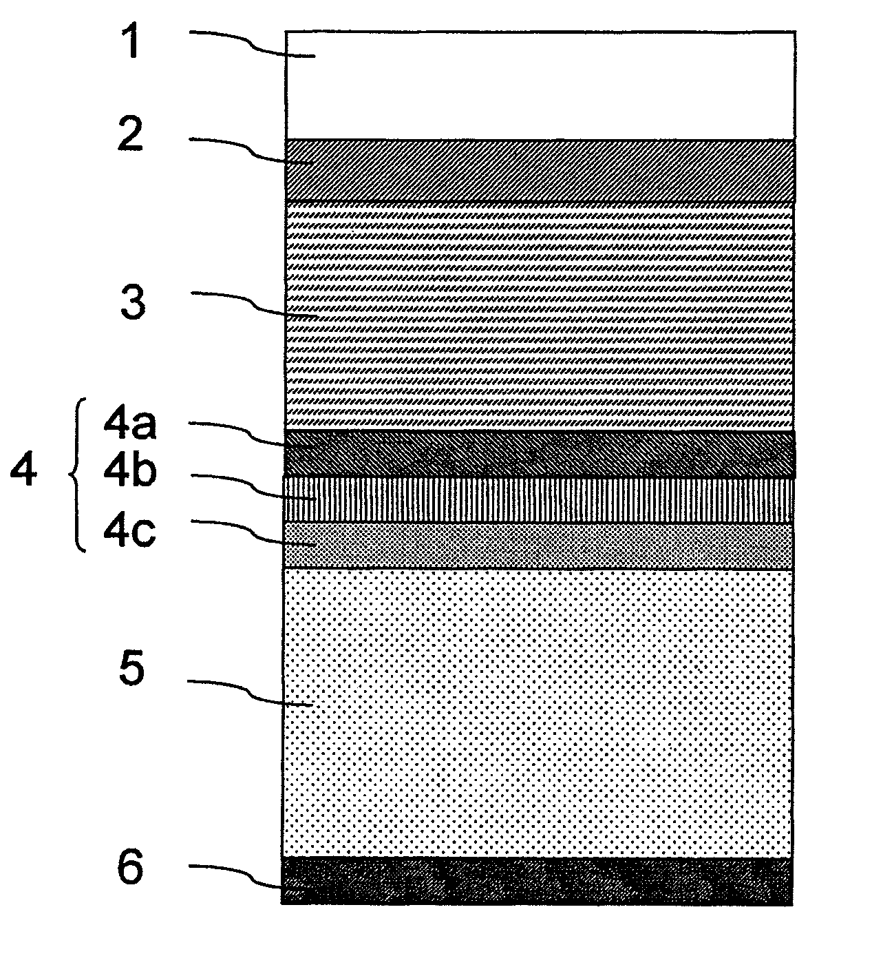
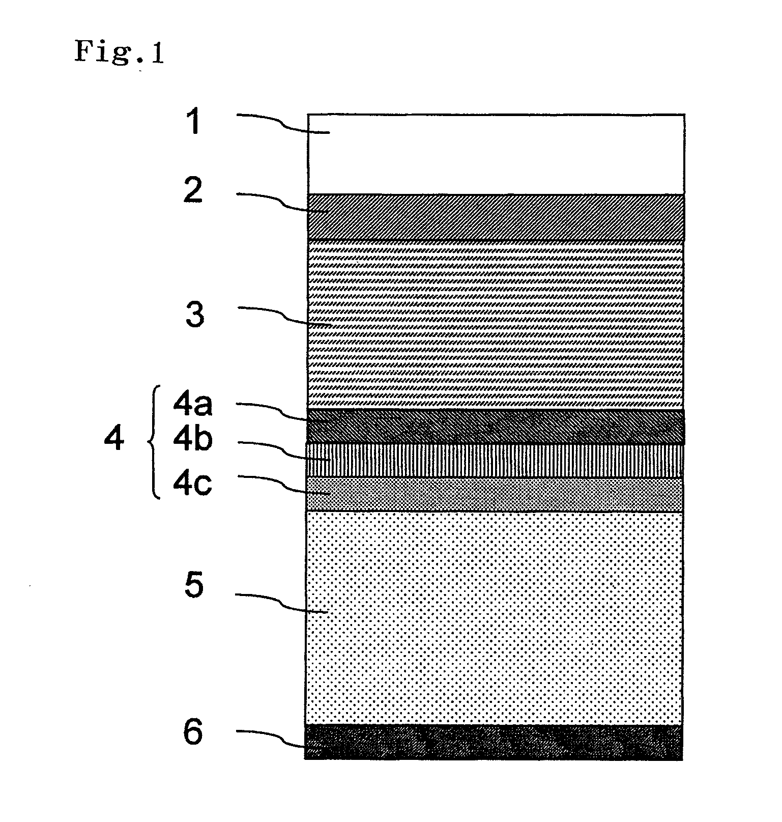
[0132]A multi-junction silicon solar cell of Example 1, which corresponds to a first embodiment described with reference to FIG. 1, was produced. Glass was used for a transparent substrate 1 and SnO2 was used for a transparent electrode layer 2. The film thickness of the transparent electrode layer 2 was 800 nm, the sheet resistance was 10Ω / □, and the haze ratio was 15 to 20%. A boron-doped p-type silicon carbide (SiC) layer, an undoped amorphous silicon photoelectric conversion layer, and a phosphorus-doped n-type μc-Si layer having thicknesses of 10 nm, 300 nm, and 20 nm, respectively were formed thereon by a plasma enhanced CVD method. Thus, a pin junction amorphous silicon photoelectric conversion unit 3 as a front photoelectric conversion unit was formed.

[0133]Further, an interlayer 4 was formed on the amorphous silicon photoelectric conversion unit 3. First, a substrate with the amorphous silicon photoelectric conversion unit 3 formed was taken out of the plasma enhanced CVD d...

example 2

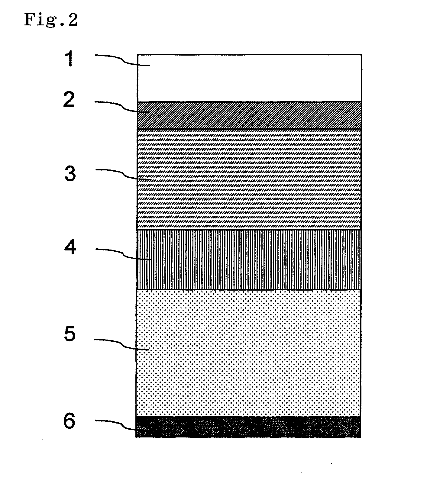
[0138]A multi-junction silicon solar cell of Example 2, which corresponds to a first embodiment described with reference to FIG. 1, was produced. The solar cell of Example 2 corresponds to a first embodiment described by referring to FIG. 1. Glass was used for a transparent substrate 1 and SnO2 was used for a transparent electrode layer 2. The film thickness of the transparent electrode layer 2 was 800 nm, the sheet resistance was 10Ω / □, and the haze ratio was 15 to 20%.

[0139]A boron-doped p-type silicon carbide (SiC) layer, an undoped amorphous silicon photoelectric conversion layer, and a phosphorus-doped n-type μc-Si layer having thicknesses of 10 nm, 300 nm, and 20 nm, respectively were formed thereon by a plasma enhanced CVD method. Thus, a pin junction amorphous silicon photoelectric conversion unit 3 as a front photoelectric conversion unit was formed.

[0140]Further, an interlayer 4 was formed on the amorphous silicon photoelectric conversion unit 3. First, a substrate with th...

example 3

[0145]A multi-junction thin-film silicon solar cell with a configuration shown in FIG. 1 was produced as Example 3. This Example was different from Example 1 only in the forming conditions of the carbon layer 4b in the interlayer 4. More specifically, in the Example 3, the substrate was placed in a plasma enhanced CVD device for forming a carbon layer 4b by a CVD method. A carbon film having a film thickness of 1000 Å was formed by using a plasma enhanced CVD device. Methane of 10 sccm (a methane concentration of 100% by volume) and hydrogen of 200 sccm were used as a raw material, a substrate temperature was 150° C., and a discharge power was 200 W.

[0146]A refractive index of the carbon layer 4b was measured by a spectroscopic ellipsometry method, and was determined to be 1.90 at a wavelength of 600 nm. In addition, the spectrum of the carbon layer was measured by using an FT-IR spectrometer. A peak derived from C—H stretching vibration was observed at approximately 2920 cm−2 in th...


PUM

PropertyMeasurementUnit
refractive indexaaaaaaaaaa

Abstract

This invention intends to develop a technique for forming an interlayer with excellent optical characteristics and to provide a photoelectric conversion device having high conversion efficiency. To realize this purpose, a series connection through an intermediate layer is formed in the thin-film photoelectric conversion device of the invention, and the interlayer is a transparent oxide layer in its front surface and n pairs of layers stacked therebehind (n is an integer of 1 or more), wherein each of the pair of layers is a carbon layer and a transparent oxide layer stacked in this order. Film thicknesses of each layer are optimized to improve wavelength selectivity and stress resistance while keeping the series resistance.
An embodiment of the photoelectric conversion device is characterized in that; a transparent insulating substrate is located on the light incidence side, and a transparent conductive layer, at least one photoelectric conversion unit, a transparent electrode layer having electrical conductivity as typified by zinc oxide, a hard carbon layer having electrical conductivity as typified by diamond-like carbon, and a high reflecting electrode layer are stacked in this order on an opposite surface from a light incidence side of the transparent insulating substrate.

Description

TECHNICAL FIELD[0001]The present invention relates to a thin-film photoelectric conversion device having an interlayer. In addition, the invention relates to an improvement in a back face electrode layer of a thin-film photoelectric conversion device.BACKGROUND ART[0002]A photoelectric conversion device for converting light into electricity by using photoelectric effect performed inside a semiconductor has been spotlighted and vigorously developed in recent years. Among the photoelectric conversion devices, a silicon-based thin-film photoelectric conversion device may be expected for lower cost by reason of being formed on a glass substrate or a stainless-steel substrate with large area at low temperature.[0003]The thin-film photoelectric conversion device generally includes a first electrode, one or more semiconductor thin-film photoelectric conversion units, and a second electrode laminated sequentially on a substrate with an insulating surface. The photoelectric conversion unit g...

Claims


Application Information

Patent Timeline
Patent Type & Authority Applications(United States)
IPC IPC(8): H01L31/00
CPCH01L31/02168H01L31/056H01L31/03682H01L31/03762H01L31/03765H01L31/0725H01L31/0745H01L31/075H01L31/076H01L31/1804H01L31/1812H01L31/202Y02E10/548Y02E10/52Y02E10/546Y02E10/547H01L31/022466H01L31/077H01L31/078Y02P70/50
Inventor MEGURO, TOMOMIICHIKAWA, MITSURUSEZAKI, FUMIYASUYOSHIKAWA, KUNTAKUCHIYAMA, TAKASHIYAMAMOTO, KENJI
Owner KANEKA CORP
Why Eureka
Try Eureka