Method for manufacturing group iii nitride semiconductor, method for manufacturing group iii nitride semiconductor light-emitting device, group iii nitride semiconductor light-emitting device, and lamp

a technology of nitride semiconductor and manufacturing group, which is applied in the direction of polycrystalline material growth, crystal growth process, vacuum evaporation coating, etc., can solve the problems of lowering production yield, extremely reducing formation rate, and not commercially available iii nitride semiconductor, so as to improve the initial dislocation loop, reduce the dislocation density of crystals, and increase the crystal film formation rate

Active Publication Date: 2010-12-02
TOYODA GOSEI CO LTD
View PDF48 Cites 18 Cited by
  • Summary
  • Abstract
  • Description
  • Claims
  • Application Information

AI Technical Summary

Benefits of technology

[0025]According to the method for manufacturing a Group III nitride semiconductor of the present invention, firstly, a substrate temperature is set to a high temperature, to thereby generate migration. Thus, the loop of initial dislocation is enhanced, and the dislocation density of a crystal is reduced. The film formation is performed in this condition, and thereafter, the film formation rate of a crystal is increased by setting a substrate temperature to a low temperature. Thus, a film having a desired thickness can be formed in a short time. Consequently, a crystal of a Group III nitride semiconductor having excellent crys

Problems solved by technology

Meanwhile, hitherto, a single crystal wafer of a Group III nitride semiconductor has not been commercially available, and Group III nitride semiconductors are, in general, produced by growing a crystal on a single crystal waf

Method used


Image

  • Method for manufacturing group iii nitride semiconductor, method for manufacturing group iii nitride semiconductor light-emitting device, group iii nitride semiconductor light-emitting device, and lamp
  • Method for manufacturing group iii nitride semiconductor, method for manufacturing group iii nitride semiconductor light-emitting device, group iii nitride semiconductor light-emitting device, and lamp
  • Method for manufacturing group iii nitride semiconductor, method for manufacturing group iii nitride semiconductor light-emitting device, group iii nitride semiconductor light-emitting device, and lamp

Examples


example 1

[0178]In Example 1, according to the following procedure, the buffer layer 12 was formed on the substrate 11 by using the reactive sputtering method, and then the GaN layer (ground layer 14a) was formed thereon by using the reactive sputtering method.

[Formation of Buffer Layer]

[0179]At first, the substrate 11 made of sapphire having a (0001) c plane of a diameter of 2 inches, the surface of which had been mirror finished, was washed with hydrofluoric acid or organic solvent, and was then introduced into a chamber of a sputtering apparatus. Here, as the sputtering apparatus, there was employed an apparatus having a high frequency-type power supply, and a mechanism capable of moving a position influenced by the magnetic field, through rotation of a magnet within a target.

[0180]The substrate 11 was heated to 500° C. in the chamber of the sputtering apparatus, into which a nitrogen gas was introduced at a flow rate of 15 sccm. Then, while keeping the pressure in the chamber at 1.0 Pa an...

example 2

[0193]In Example 2, according to the following procedure, the buffer layer 12 was formed on the substrate 11 using the sputtering apparatus 40 shown in FIG. 5, and then the ground layer 14a made of GaN was formed thereon.

[0194]In present Example, firstly, the buffer layer 12 made of AlN having a single-crystalline structure was formed on the c plane of the substrate 11 made of sapphire using the sputtering apparatus 40 according to the same procedure as in Example 1. The ground layer 14a of the n-type semiconductor layer 14 made of the undoped GaN layer was formed thereon.

[0195]Firstly, the substrate 11 formed with the buffer layer 12 was removed from the chamber of the sputtering apparatus and transported into the chamber 41 of the sputtering apparatus 40 as represented by FIG. 5. As the sputtering apparatus 40 for use in the formation of the ground layer 14a of the n-type semiconductor layer 14, there was employed a sputtering apparatus in which the target 47 was made of a metal G...

example 3

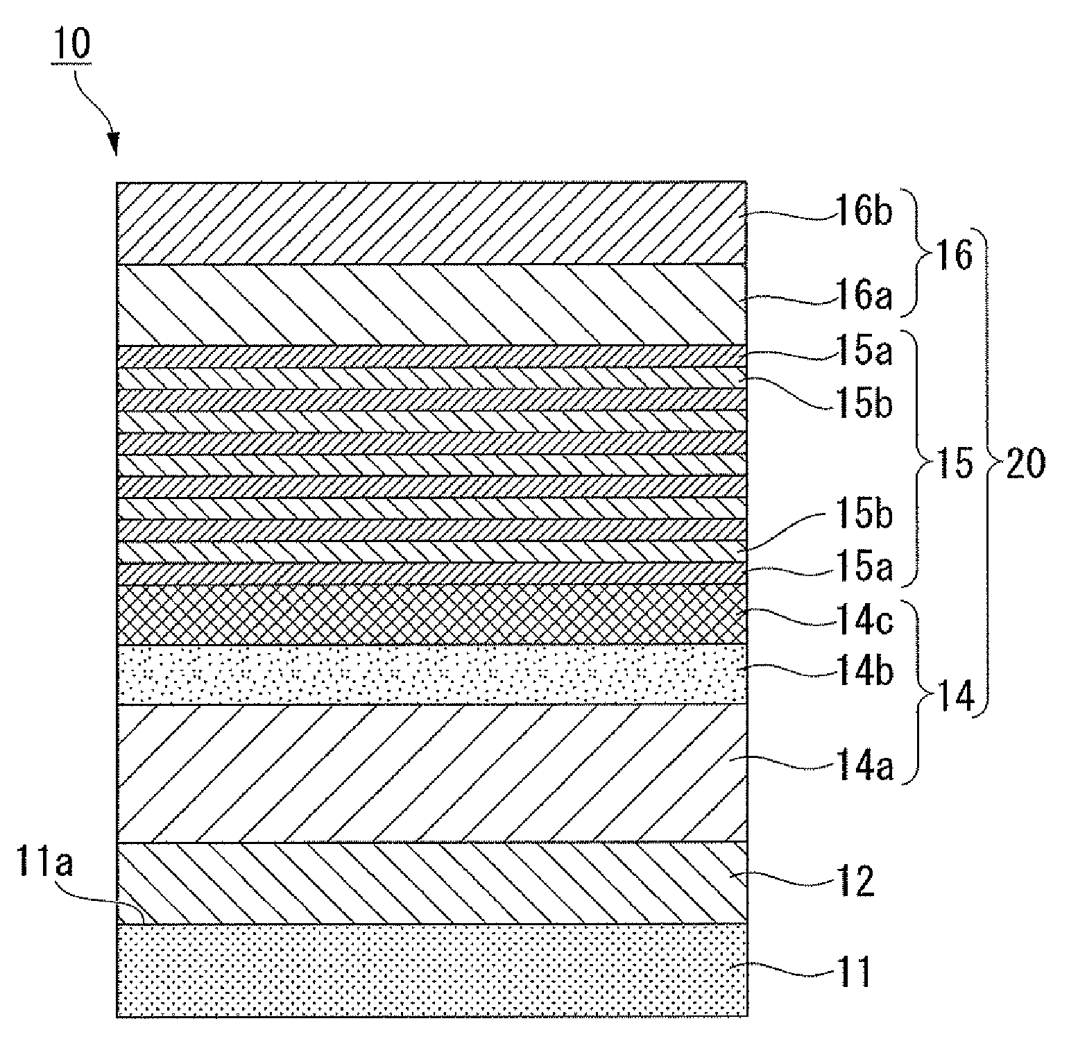
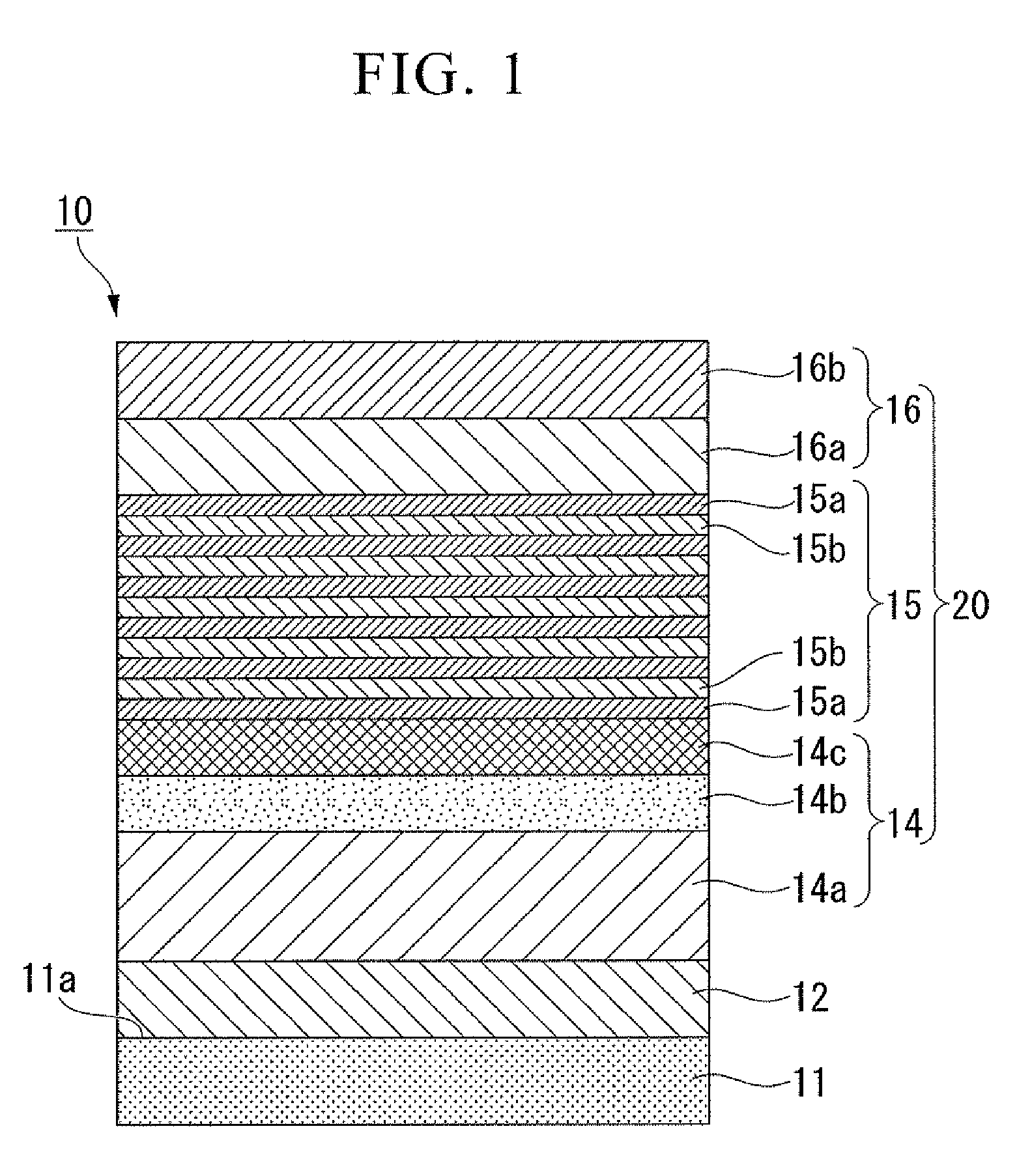
[0204]In Example 3, according to the same procedure as in Example 2, the buffer layer 12 was formed on the substrate 11, and then the ground layer 14a made of GaN was formed thereon. In addition, the respective layers were formed thereon according to the following procedure, to thereby produce the laminated semiconductor 10 represented by FIG. 1. Moreover, the transparent electrode 17, the positive electrode bonding pad 18, and the negative electrode 19 were formed for the laminated semiconductor 10, to thereby produce the light-emitting device 1 represented by FIGS. 2 and 3.

[Formation of N-Type Contact Layer]

[0205]According to the same procedure as in Example 2, the substrate 11 formed with the buffer layer 12 and the ground layer 14a was transported from the sputtering apparatus 40 into the chamber 41 of the other sputtering apparatus 40 having the same structure. As the sputtering apparatus 40 for use in the formation of the n-type contact layer 14b, there was employed the sputte...


PUM

PropertyMeasurementUnit
Temperatureaaaaaaaaaa

Abstract

A method for manufacturing a Group III nitride semiconductor of the present invention includes a sputtering step of forming a single-crystalline Group III nitride semiconductor on a substrate by a reactive sputtering method in a chamber in which a substrate and a Ga element-containing target are disposed, wherein said sputtering step includes respective substeps of: a first sputtering step of performing a film formation of the Group III nitride semiconductor while setting the temperature of the substrate to a temperature T1; and a second sputtering step of continuing the film formation of the Group III nitride semiconductor while lowering the temperature of the substrate to a temperature T2 which is lower than the temperature T1.

Description

TECHNICAL FIELD[0001]The present invention relates to a method for manufacturing a Group III nitride semiconductor which is suitably used for a light emitting diode (LED), a laser diode (LD), an electronic device, and the like, and represented by the general formula AlaGabIncN (0≦a≦1, 0≦b≦1, 0≦c≦1, and a+b+c=1); a method for manufacturing a Group III nitride semiconductor light-emitting device; a Group III nitride semiconductor light-emitting device; and a lamp.[0002]Priority is claimed on Japanese Patent Application No. 2007-308823, filed Nov. 29, 2007, the content of which is incorporated herein by reference.BACKGROUND ART[0003]Group III nitride semiconductors offer a direct transition over a band gap energy from visible light to ultraviolet rays, and excel in the light emission efficiency, and thus have been manufactured as semiconductor light-emitting devices such as a light emitting diode (LED) and a laser diode (LD) for use in various applications. In addition, when used for a...

Claims


Application Information

Patent Timeline
IPC IPC(8): H01L33/30H01L33/02C23C14/34H01L33/06
CPCC30B23/02H01L2224/45144H01L21/0237H01L21/0242H01L21/02458H01L21/0254H01L21/02573H01L21/0262H01L21/02631H01L33/007H01L33/06H01L2924/1305H01L2224/48091H01L2224/48247H01L2224/49107H01L2224/73265C30B29/403H01L2924/00014H01L2924/00H01L2924/181H01L2924/30111H01L2924/00012
Inventor YOKOYAMA, YASUNORIMIKI, HISAYUKI
Owner TOYODA GOSEI CO LTD
Why Eureka
Try Eureka