
Photoelectric conversion device and imaging device

a conversion device and imaging device technology, applied in thermoelectric devices, solid-state devices, nano-informatics, etc., can solve the problems of severely restricted structure, achieve high photoelectric conversion efficiency, high charge transportability, and high speed response

Active Publication Date: 2010-12-09
FUJIFILM CORP
View PDF12 Cites 8 Cited by
  • Summary
  • Abstract
  • Description
  • Claims
  • Application Information

AI Technical Summary

Benefits of technology

[0017]In the case of providing a charge blocking layer as in Patent Document 2, the charge blocking layer is required to have not only a blocking ability but also high charge transportability so as to realize high photoelectric conversion efficiency and high-speed response.
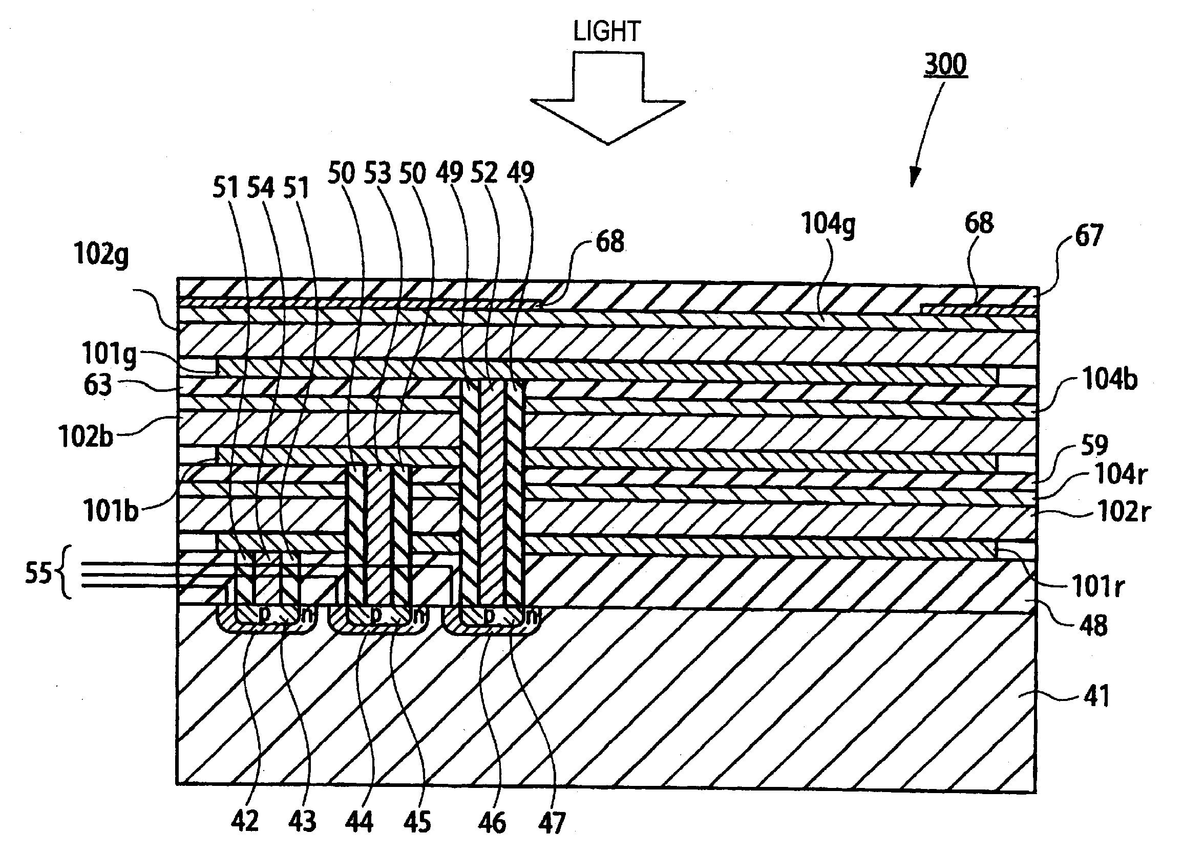
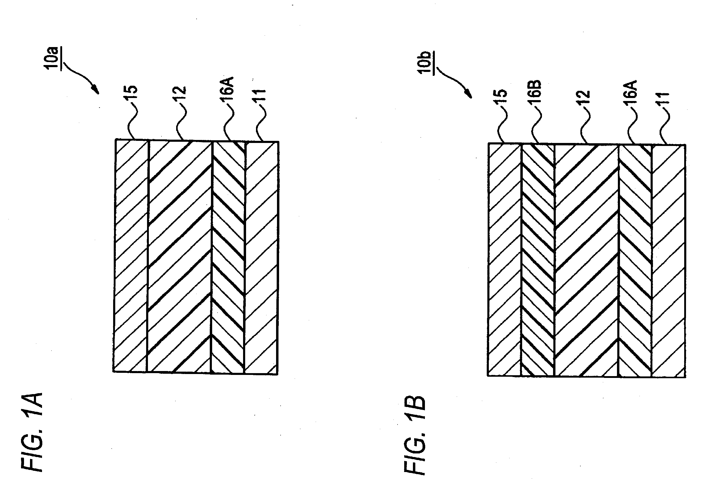
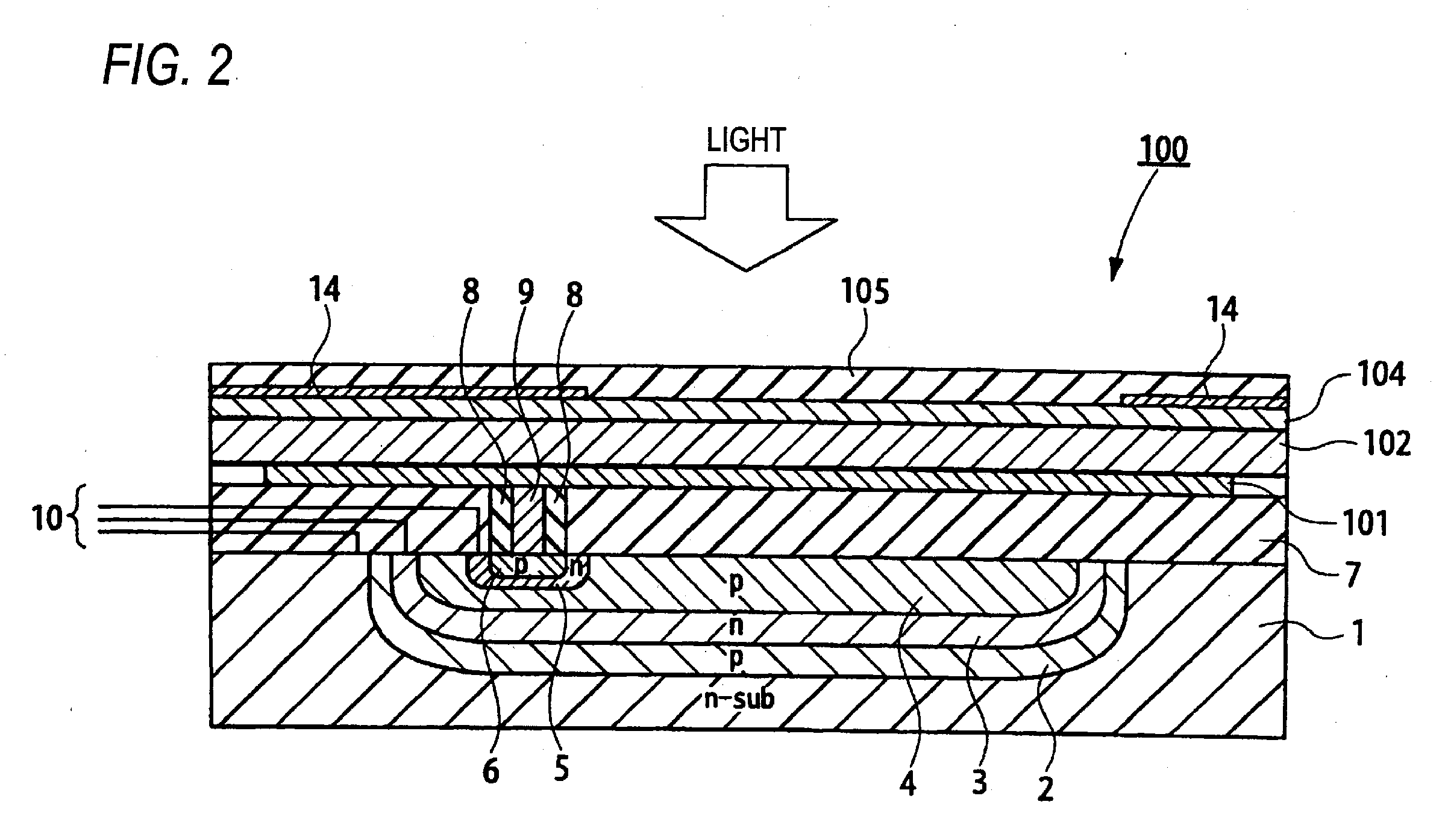
[0023]The present invention has been made to solve these problems, and an object of the present invention is to provide a photoelectric conversion device capable of suppressing a source charge (electron, hole) produced at the interface between different materials in a photoelectric conversion film and effectively decreasing the dark current, and an imaging device equipped with such a photoelectric conversion device.
[0024]As a result of intensive studies, the present inventors have found that in a photoelectric conversion device having a photoelectric conversion film containing a material with large Ea, when a compound represented by the following formula is used for the material (layer) coming into contact with the material having large Ea, a source charge (electron, hole) produced at the interface between the material having large Ea and a material (layer) in contact therewith can be suppressed to an extent of effectively reducing the dark current and causing no problem in practice by heating. The compound represented by the following formula has a high effect of reducing the dark current as compared with conventional materials having the same Ip and therefore, the allowable Ip can be smaller, increasing the alternative of substituents usable in the molecular structure, so that the freedom of molecular design can be enhanced.
[0045]According to the present invention, a photoelectric conversion device and an imaging device, which are capable of suppressing a source charge (electron, hole) produced at the interface between different materials in a photoelectric conversion film and effectively decreasing the dark current, can be provided.

Problems solved by technology

That is, in the case of forming a charge blocking layer, for example, forming an electron blocking layer, the material needs to be designed to satisfy low Ea (electron affinity), high hole transportability, high heat resistance and the like, and the structure is severely restricted so as to satisfy these requirements.

Method used


Image

  • Photoelectric conversion device and imaging device
  • Photoelectric conversion device and imaging device
  • Photoelectric conversion device and imaging device

Examples


synthesis example 1

[0349]Benz[f]indane-1,3-dione was synthesized according to J. Med. Chem., Vol. 16, paragraphs 1334 to 1339 (1973), and 2 g of this sample and 3.1 g of 4-(N,N-diphenylamino)benzaldehyde were heated with stirring in 20 ml of ethanol under reflux for 6 hours. After cooling to room temperature, the obtained crystal was separated by filtration, washed and recrystallized from chloroform-acetonitrile to obtain 4.3 g of Compound (1).

synthesis example 2

[0350]9H-Tribenz[b,d,f]azepine was synthesized according to J. Org. Chem., Vol. 56, paragraphs 3906 to 3908 (1991), and 3.2 g of this sample, 2 g of 2,6-dibromoanthracene, 1.4 g of tert-butoxysodium, 50 ml of xylene and 250 mg of bis(tri-tert-butylphosphine)palladium(0) were refluxed for 5 hours under nitrogen. After cooling to room temperature, 150 ml of methanol was added, and the obtained crystal was filtered, washed with acetonitrile and dispersed in 30 ml of toluene and 50 ml of water, and the dispersion was stirred for 1 hour, filtered and washed sequentially with acetonitrile and with toluene to obtain 4.2 g of Compound (6).

synthesis example 3

[0351]3,6-Di-tert-butylcarbazole was synthesized according to ORGANIC LETTERS, Vol. 9, paragraphs 797 to 800 (2007), and 3.3 g of this sample, 0.2 g of palladium acetate, 9 g of cesium carbonate, 1 g of tri-tert-butylphosphine, 50 ml of xylene and 5 g of 3,6-dibromo-9-phenylcarbazole were refluxed for 5 hours under nitrogen. After cooling to room temperature, 100 ml of water was added, and extraction with 100 ml of toluene was performed. The concentrated residue was purified by silica gel column chromatography using a toluene-hexane mixed solvent, and the solution was concentrated. Thereafter, 50 ml of methanol was added to the residue, and the obtained crystal was filtered and washed with acetonitrile to obtain 6 g of Compound (2).


PUM


Abstract

Provided is a photoelectric conversion device comprising a transparent electrically conductive film, a photoelectric conversion film, and an electrically conductive film, wherein the photoelectric conversion film contains a compound represented by the following formula (i):wherein each of R2 to R9 independently represents a hydrogen atom or a substituent, provided that each of at least two out of R3, R4, R7 and R8 independently represents an aryl group, a heterocyclic group or —N(Ra)(Rb), each of Ra and Rb independently represents a hydrogen atom or a substituent, and at least either Ra or Rb represents an aryl group or a heterocyclic group; and R1 represents an alkyl group, an aryl group or a heterocyclic group.

Description

BACKGROUND OF THE INVENTION[0001]1. Field of the Invention[0002]The present invention relates to a photoelectric conversion device and an imaging device.[0003]2. Description of the Related Art[0004]As for the solid-state imaging device, there is widely used a flat light-receiving device where photoelectric conversion sites are two-dimensionally arrayed in a semiconductor to form pixels and a signal generated by photoelectric conversion in each pixel is charge-transferred and read out according to a CCD or CMOS format. The conventional photoelectric conversion site is generally formed, for example, by forming PN junction in a semiconductor such as Si.[0005]In recent years, with the progress of a multi-pixel system, the pixel size and in turn, the area of a photodiode part becomes small, and this brings about problems of reduction in the aperture ratio and reduction in the light gathering efficiency. As for the measure to enhance the aperture ratio and the like, studies are being made...

Claims


Application Information

Patent Timeline
IPC IPC(8): H01L51/46
CPCB82Y10/00H01L51/0046H01L51/0058Y02E10/549H01L51/0072H01L51/4246H01L51/4253H01L51/0059H10K85/211H10K85/631H10K85/626H10K85/6572H10K30/30H10K39/32H10K30/211
Inventor MITSUI, TETSURONOMURA, KIMIATSUYOFU, KATSUYUKI
Owner FUJIFILM CORP
Learn More