Oxide semiconductor target and manufacturing method of oxide semiconductor device by using the same

a manufacturing method and semiconductor technology, applied in the direction of electrolysis components, vacuum evaporation coatings, coatings, etc., can solve the problems of difficult application as thin film transistors, lack of versatility of oxide semiconductor materials such as izo, izo, izo, etc., and achieve the effect of less restriction, high mobility and threshold potential stability

Inactive Publication Date: 2010-12-30
HITACHI METALS LTD
View PDF6 Cites 39 Cited by
  • Summary
  • Abstract
  • Description
  • Claims
  • Application Information

AI Technical Summary

Benefits of technology

[0022]According to the method described above, it is possible to provide an appropriate Zn/(Zn+Sn) composition for a ZTO (zinc tin complex oxide) type oxide semiconductor material having high mobility and threshold potential stability, and with less restriction in view of the cost and the resource and less restriction

Problems solved by technology

However, in a-Si used mainly for the switching of existent liquid crystal displays, since the threshold potential shift greatly exceeds about 2V which is controlled easily by a compensation circuit, it is considered that this is

Method used


Image

  • Oxide semiconductor target and manufacturing method of oxide semiconductor device by using the same
  • Oxide semiconductor target and manufacturing method of oxide semiconductor device by using the same
  • Oxide semiconductor target and manufacturing method of oxide semiconductor device by using the same

Examples


first embodiment

[0059]A first embodiment is to be described with reference to FIG. 5 to FIG. 7, and FIG. 8A to FIG. 8E. Those described in the column in preferred embodiments of the invention and not described in this embodiment are identical with those for the description of preferred embodiments of the invention.

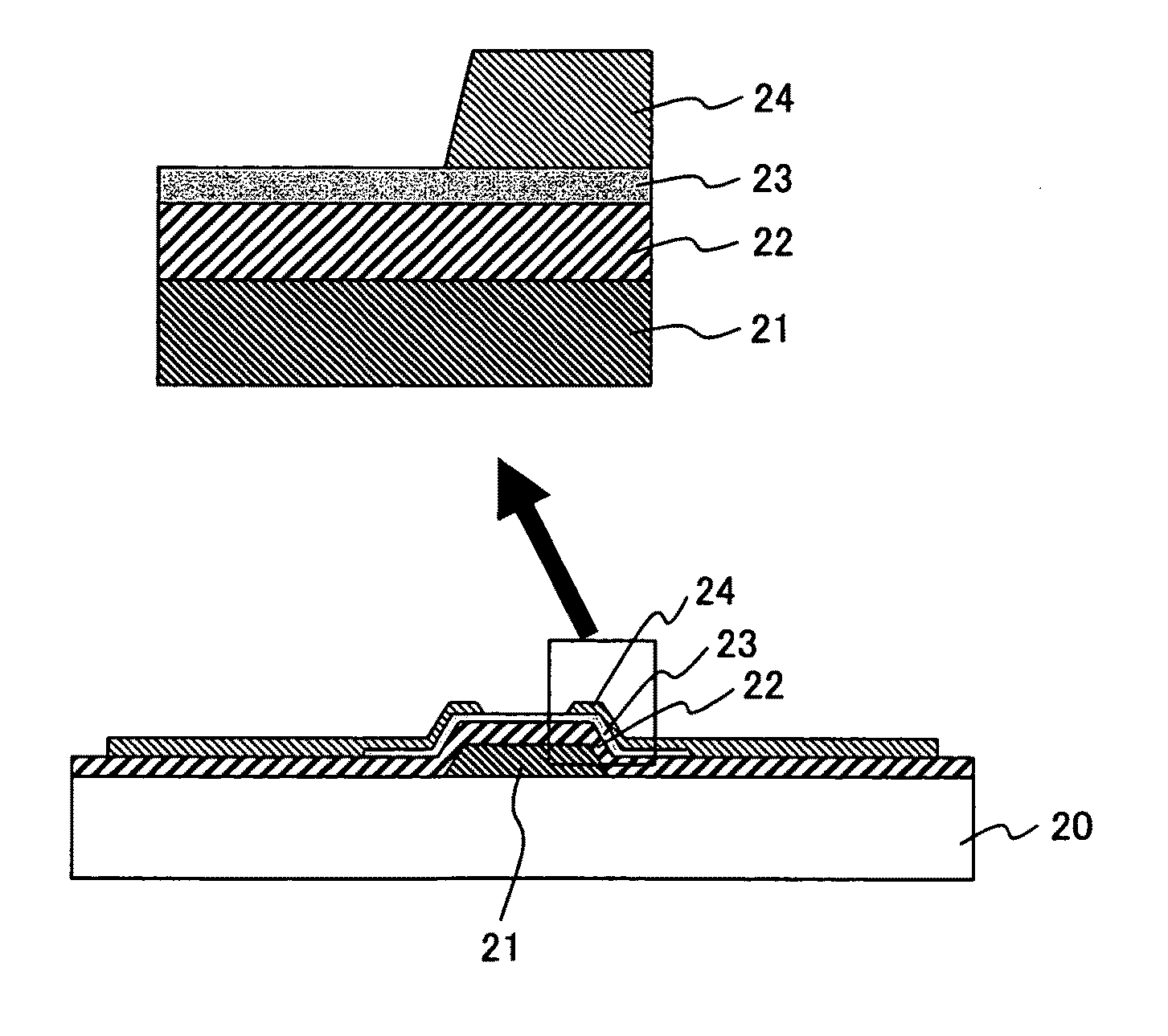
[0060]FIG. 5 is a photograph showing the difference of appearance between a sputtering target for a semiconductor and a sputtering target for a transparent electrode according to this embodiment. FIG. 6 is a schematic view of an RF sputtering apparatus applied with a sputtering target according to this embodiment, and FIG. 7 is a cross sectional view showing the structure of a thin film transistor utilizing the oxide semiconductor channel layer formed by applying the sputtering target according to this embodiment (upper view is a fragmentary cross sectional view). FIG. 8A to FIG. 8E are flow charts showing the method of manufacturing the thin film transistor.

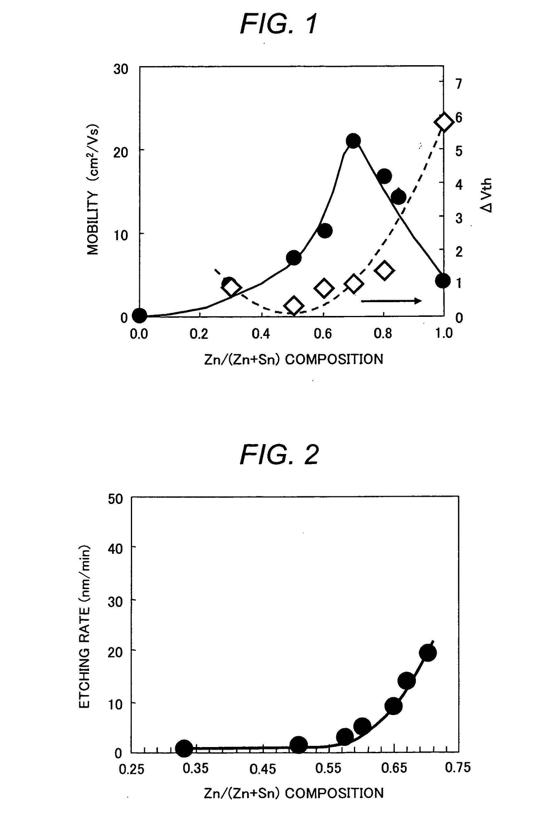
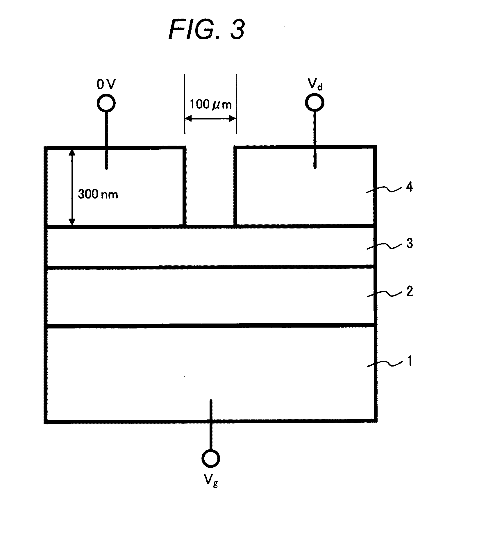
[0061]A method of manufacturin...

second embodiment

[0073]A second embodiment is to be described with reference to FIGS. 9 to 10. Matters described in the preferred embodiments of the invention, or those described in the first embodiment and not described in this embodiment are identical with those described in the preferred embodiment of the invention and in the first embodiment.

[0074]FIG. 9 is a schematic view of an electron beam vapor deposition apparatus using a low density oxide target according to this embodiment as an evaporation source. There are shown an evaporation source 30, an oxide target 31, an electron beam source 32, an ion source 33 (for ion assisting), a substrate holder 34, a substrate swinging device 35, a mass flow controller 36, a cryopump or molecule turbo pump 37, and a dry pump or rotary pump 38.

[0075]FIG. 10 is a cross sectional view showing a portion of a basic structure of an organic EL display using a thin film transistor manufactured by using an oxide semiconductor target according to this embodiment for...

third embodiment

[0083]A third embodiment is to be described with reference to FIGS. 11 to 14. Matters described in the preferred embodiments of the invention, or those described in the first embodiment and not described in this embodiment are identical with those described in the preferred embodiments of the invention and in the first embodiment.

[0084]FIG. 11 is a cross sectional view of a one time programmable memory cell having a bottom gate top contact type thin film transistor formed by using the ZTO target according to the first embodiment or the second embodiment as a basic structure, FIG. 12 is a configurational view of an oxide semiconductor memory according to this embodiment, FIG. 13 is a bird's-eye view of an carry for oxide semiconductor thin film transistors according to this embodiment, FIG. 14A is a circuit diagram of a programmable using oxide semiconductor thin film transistor memory device and incorporated with a capacitor element on the side of a drain electrode, FIG. 14B is a cr...


PUM

PropertyMeasurementUnit
Fractionaaaaaaaaaa
Fractionaaaaaaaaaa
Electrical resistivityaaaaaaaaaa

Abstract

An oxide semiconductor target of a ZTO (zinc tin complex oxide) type oxide semiconductor material of an appropriate (Zn/(Zn+Sn)) composition having high mobility and threshold potential stability and with less restriction in view of the cost and the resource and with less restriction in view of the process, and an oxide semiconductor device using the same, in which a sintered Zn tin complex oxide with a (Zn/(Zn+Sn)) composition of 0.6 to 0.8 is used as a target, the resistivity of the target itself is at a high resistance of 1 Ωcm or higher and, further, the total concentration of impurities is controlled to 100 ppm or less.

Description

CLAIM OF PRIORITY[0001]The present application claims priority from Japanese patent application JP 2009-096937 filed on Apr. 13, 2009, the content of which is hereby incorporated by reference into this application.BACKGROUND OF THE INVENTION[0002]1. Field of the Invention[0003]The present invention concerns an oxide semiconductor target material for depositing an oxide semiconductor material and it particularly relates to a material technique of a sintered body target used for sputtering. Further, the invention also includes a technique relating to a method of manufacturing an oxide semiconductor thin film transistor manufactured by using the target material and utilized as a switching device for a liquid crystal display or an organic EL display.[0004]2. Description of the Related Art[0005]In recent years, display devices have been developed rapidly from display using a cathode ray tube to a planar type display device referred to as a flat panel display (FPD) such as a liquid crysta...

Claims


Application Information

Patent Timeline
IPC IPC(8): H01L21/36C23C14/35C23C14/34H01L21/365
CPCC04B35/453H01L29/66969C04B2235/3284C04B2235/3293C04B2235/6585C04B2235/72C04B2235/722C04B2235/727C04B2235/77C23C14/086C23C14/3414H01L21/02554H01L21/02565H01L21/02631H01L29/7869C04B35/457
Inventor UCHIYAMA, HIROYUKIWAKANA, HIRONORIKAWAMURA, TETSUFUMIKURITA, FUMIFUKUSHIMA, HIDEKO
Owner HITACHI METALS LTD
Why Eureka
Try Eureka