Eureka AIR delivers breakthrough ideas for toughest innovation challenges, trusted by R&D personnel around the world.

Electron donating material, material for photovoltaic devices and photovoltaic device

a technology of organic materials and electron donors, applied in the direction of solid-state devices, organic chemistry, chemistry apparatus and processes, etc., can solve the problems of low photoelectric conversion efficiency of solar cells, high cost mainly derived from the process of producing semiconductor films, and inability to spread widely to homes, etc., to achieve high short-circuit current density (isc), high photoelectric conversion efficiency, and high open-circuit voltage

Inactive Publication Date: 2011-02-03
TORAY IND INC
View PDF3 Cites 21 Cited by
  • Summary
  • Abstract
  • Description
  • Claims
  • Application Information

AI Technical Summary

Benefits of technology

[0011]It is thus possible to provide a photovoltaic device with high photoelectric conversion efficiency, which achieves a high short-circuit current density (Isc) and a high open circuit voltage (Voc) simultaneously.

Problems solved by technology

However, solar cells produced using inorganic semiconductors have not spread widely for home use because of their cost higher than that of power generation systems such as thermal power generation and nuclear power generation.
Such a high cost is derived mainly from the process of producing a semiconductor film in vacuum at high temperatures.
However, the most serious problem with organic solar cells using organic semiconductors such as conjugated polymers and the like is that such solar cells are low in photoelectric conversion efficiency in comparison with solar cells using conventional inorganic semiconductors, and therefore such solar cells have not been used practically, yet.
The first reason is that solar light absorption efficiency is low.
The third reason is that since a trap which captures a carrier (electron or hole) is likely to be formed, a produced carrier tends to be captured by the trap, resulting in low mobility of carriers.
In other words, while a semiconductor material is generally required that the carriers of the material has a high mobility μ, there is a problem that conjugated polymers have mobilities μ being lower than those of conventional inorganic crystalline semiconductors or amorphous silicon.
In such devices, since only organic layers (almost several molecular layers) in a junction contribute to the generation of a photocurrent, the photoelectric conversion efficiency is low and, and therefore the improvement in the efficiency is a pending problem.
However, sufficient photoelectric conversion efficiency has not been obtained, yet.
As described above, all of such conventional organic solar cells have a problem that photoelectric conversion efficiency is low.

Method used

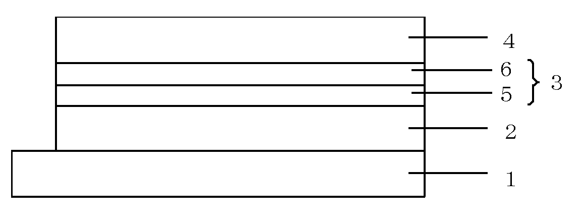
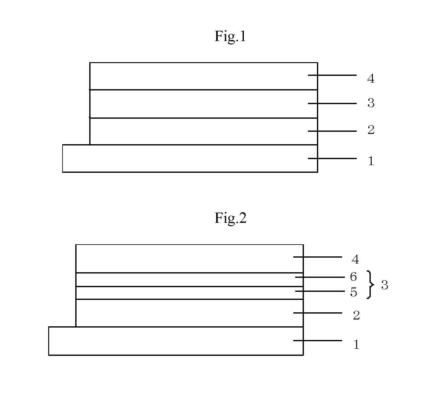

Image

  • Electron donating material, material for photovoltaic devices and photovoltaic device
  • Electron donating material, material for photovoltaic devices and photovoltaic device
  • Electron donating material, material for photovoltaic devices and photovoltaic device

Examples


synthesis example 1

[0082]Compound A-1 was synthesized by the method illustrated in Scheme 1.

[0083]To 150 ml of 48% hydrobromic acid (produced by Wako Pure Chemical Industries, Ltd.) were added 4.3 g of compound (1-a) (produced by Tokyo Chemical Industry Co., Ltd.) and 10 g of bromine (produced by Wako Pure Chemical Industries, Ltd.), and the resulting mixture was stirred at 120° C. for 3 hours. After cooling the mixture to room temperature, precipitated solid was separated by filtration by a glass filter, and then washed with 1000 ml of water and 100 ml of acetone. The resulting solid was dried in vacuum at 60° C. to obtain 6.72 g of compound (1-b).

[0084]In 100 ml of dimethylformamide (produced by Kishida Chemical Co., Ltd.) was dissolved 10.2 g of compound (1-c) (produced by Tokyo Chemical Industry Co., Ltd.), and then 9.24 g of N-bromosuccinimide (produced by Wako Pure Chemical Industries, Ltd.) was added, and the resulting mixture was stirred under a nitrogen atmosphere at room temperature for 3 ho...

synthesis example 2

[0091]Compound A-2 was synthesized by the method illustrated in Scheme 2.

[0092]In 15 ml of chloroform (produced by NACALAI TESQUE, Inc.) was dissolved 0.734 g of the compound A-1 (produced by Tokyo Chemical Industry Co., Ltd.), and then 0.23 g of N-bromosuccinimide (produced by Tokyo Chemical Industry Co., Ltd.) / 10 ml of dimethylformamide (produced by Wako Pure Chemical Industries, Ltd.) were added, and the resulting mixture was stirred under a nitrogen atmosphere at room temperature for 9 hours. To the resulting solution were added 100 ml of water and 100 ml of chloroform. Then, an organic layer was fractionated, washed with 200 ml of water, and then dried with magnesium sulfate. The resulting solution was purified by column chromatography (filler: silica gel, eluent: dichloromethane / hexane) to obtain 0.58 g of compound (2-a).

[0093]To 7 ml of 1,4-dioxane (produced by Wako Pure Chemical Industries, Ltd.) were added 0.5 g of compound (2-b) (produced by Tokyo Chemical Industry Co., Lt...

synthesis example 3

[0095]Compound A-3 was synthesized by the method illustrated in Scheme 3.

[0096]To 7 ml of 1,4-dioxane (produced by Wako Pure Chemical Industries, Ltd.) were added 0.34 g of compound (3-a) (produced by Tokyo Chemical Industry Co., Ltd.), 0.85 g of bis(pinacolato)diboron (produced by BASF Japan Ltd.) and 0.86 g of potassium acetate (produced by Wako Pure Chemical Industries, Ltd.). Under a nitrogen atmosphere, 0.21 g of [bis(diphenylphosphino)ferrocene]dichloropalladium (produced by Aldrich Chemical Company, Inc.) was added and the resulting mixture was stirred at 80° C. for 9 hours. To the resulting solution were added 100 ml of water and 100 ml of ethyl acetate. Then, an organic layer was fractionated, washed with 100 ml of water, and then dried with magnesium sulfate. The resulting solution was purified by column chromatography (filler: silica gel, eluent: dichloromethane) to obtain 167 mg of compound (3-b).

[0097]In 6 ml of toluene were dissolved 110 mg of the compound (2-a) and 17...


PUM

PropertyMeasurementUnit
Energyaaaaaaaaaa
Energyaaaaaaaaaa
Nanoscale particle sizeaaaaaaaaaa

Abstract

An electron donating organic material includes a benzothiadiazole compound including (a) a benzothiadiazole skeleton and (b) an oligothiophene skeleton, and having a band gap (Eg) of 1.8 eV or less, and a level of highest occupied molecular orbital (HOMO) of −4.8 eV or less, wherein said benzothiadiazole compound is formed by covalently combining the benzothiadiazole skeleton and the oligothiophene skeleton alternately, a proportion between the benzothiadiazole skeleton and the oligothiophene skeleton is within a range of 1:1 to 1:2 (however, excluding 1:1), and the number of thiophene rings contained in an oligothiophene skeleton is 3 or more and 12 or less.

Description

RELATED APPLICATIONS[0001]This is a §371 of International Application No. PCT / JP2009 / 054836, with an international filing date of Mar. 13, 2009, which is based on Japanese Patent Application Nos. 2008-103205 filed Apr. 11, 2008 and 2008-271688 filed on Oct. 22, 2008, the subject matter of which is incorporated by reference.TECHNICAL FIELD[0002]This disclosure relates to an electron donating organic material, a material for photovoltaic devices and a photovoltaic device using the same.BACKGROUND ART[0003]Solar cells have been attracting attention as an environment-friendly electric energy source. Now, inorganic substances, such as monocrystalline silicon, polycrystalline silicon, amorphous silicon and compound semiconductor, are used as a semiconductor material of a photovoltaic device of a solar cell. However, solar cells produced using inorganic semiconductors have not spread widely for home use because of their cost higher than that of power generation systems such as thermal powe...

Claims


Application Information

Patent Timeline
IPC IPC(8): H01L51/46C08G75/32
CPCC07D417/14C07F7/0812C08G61/123C08G61/126H01L51/0007Y02E10/549H01L51/0039H01L51/0043H01L51/0094H01L51/4253H01L51/0036H10K71/15H10K85/115H10K85/113H10K85/151H10K85/40H10K30/30H10K30/50C08G61/12H10K10/00
Inventor KITAZAWA, DAISUKEYAMAMOTO, SHUHEITSUKAMOTO, JUN
Owner TORAY IND INC
Why Eureka
Eureka Blog
Learn More