Making films composed of semiconductor nanocrystals

a technology of nanocrystals and polycrystalline films, which is applied in the direction of luminescent compositions, electrical devices, chemistry apparatus and processes, etc., can solve the problems of insufficient device performance for market needs, relatively high cost, and limited efficiency, and achieves low aspect ratio, high crystallinity, and large size

Inactive Publication Date: 2011-03-31
EASTMAN KODAK CO
View PDF12 Cites 10 Cited by
  • Summary
  • Abstract
  • Description
  • Claims
  • Application Information

AI Technical Summary

Benefits of technology

[0019]It is an advantage of the present invention to enable a method of forming polycrystalline films of II-VI nanocrystals having an aspect ratio less than 3:1 and a diameter greater than 10 nanometers. In accordance with the present invention, it has been determined that the use of large amount of fatty acids or phosphonic acids prevents the formation of organic-free films comprising large II-VI nanocrystals. By using the above-described coordinating solvents, the problem has been overcome and films of large II-VI nanocrystals with less than 5% by volume of organic material can now be made. Large-sized II-VI nanocrystals with high crystallinity are formed by injecting under heat a lower molar quantity of column VI chemical precursors than column II chemical precursors; then gradually increasing the ratio of column VI to column II chemical precursors during the course of the reaction. The resulting nanocrystals can be cleanly isolated from the reaction mixture. As such, polycrystalline films of large II-VI nanocrystals with less than 5% by volume of organic material are formed. The large size and low aspect ratio of the nanocrystals facilitates formation of doped semiconductor nanoparticles with modified carrier concentration. The presence of low volumes of organic materials in the films formed from these in-situ doped nanoparticles enables enhanced carrier transport in the films. By incorporating in-situ doped inorganic nanoparticles into the transport layers of electronic devices, one can produce the devices at low cost while still maintaining good device performance. In addition, the device layers can be deposited by low cost processes, such as, drop casting, spin coating, or inkjetting, and the resulting nanoparticle-based device can also be formed on a range of substrates.
to enable a method of forming polycrystalline films of II-VI nanocrystals having an aspect ratio less than 3:1 and a diameter greater than 10 nanometers. In accordance with the present invention, it has been determined that the use of large amount of fatty acids or phosphonic acids prevents the formation of organic-free films comprising large II-VI nanocrystals. By using the above-described coordinating solvents, the problem has been overcome and films of large II-VI nanocrystals with less than 5% by volume of organic material can now be made. Large-sized II-VI nanocrystals with high crystallinity are formed by injecting under heat a lower molar quantity of column VI chemical precursors than column II chemical precursors; then gradually increasing the ratio of column VI to column II chemical precursors during the course of the reaction. The resulting nanocrystals can be cleanly isolated from the reaction mixture. As such, polycrystalline films of large II-VI nanocrystals with less than 5% by volume of organic material are formed. The large size and low aspect ratio of the nanocrystals facilitates formation of doped semiconductor nanoparticles with modified carrier concentration. The presence of low volumes of organic materials in the films formed from these in-situ doped nanoparticles enables enhanced carrier transport in the films. By incorporating in-situ doped inorganic nanoparticles into the transport layers of electronic devices, one can produce the devices at low cost while still maintaining good device performance. In addition, the device layers can be deposited by low cost processes, such as, drop casting, spin coating, or inkjetting, and the resulting nanoparticle-based device can also be formed on a range of substrates.

Problems solved by technology

Most semiconductor devices in use today, both inorganic and organic, are in part or completely formed using expensive vacuum deposition processes.
There are ongoing efforts to find a low cost manufacturing process, however, device performance has been inadequate for market needs.
While these devices are useful in certain applications, their efficiency has been somewhat limited, yielding conversion efficiencies, e.g., solar power to electrical power, of typically marginally better than 10-20%.
Although efficiencies of these devices have been improving through costly improvements to device structure, the relative inefficiency of these devices, combined with their relatively high cost, have combined to inhibit the widespread adoption of solar electricity in the consumer markets.
However, the performance of these devices was not reported, and the conductivity of such a mixed photoactive layer should be low due to the high resistivity of the polymeric binder.
A large part of the low efficiency was undoubtedly due to the films being insulators (even after sintering) due to the lack of doping.
In addition, the process is inefficient with respect to usage of its starting materials.
As a result of surface plasmon effects (K. B. Kahen, Appl. Phys. Lett. 78, 1649 ), having metal layers adjacent to emitter layers results in a loss emitter efficiency.
As is well known in the art, highly doping wide bandgap semiconductors is difficult as a result of self-compensation effects.
Consequently, forming ohmic contacts to these layers can prove to be difficult.
The dominant ones are high manufacturing costs, difficulty in combining multi-color output from the same chip, and the need for high cost and rigid substrates.
However, many of these dopants are unstable and the resistivities are many orders of magnitude higher than crystalline LED values of ˜0.1 ohm-cm.
The result of employing resistive layers is that one suffers from ohmic heating effects; it is difficult to make ohmic contacts and since the drive current of the device is limited, so is the overall brightness of the device.
The above examples illustrate that higher performance semiconductor devices can be created from crystalline semiconductor materials, but with the drawback of high manufacturing costs.
Attempts to reduce the manufacturing costs by employing organic materials result in lower performance devices whose specifications sometimes fall significantly short of market requirements (e.g., organic-based photovoltaics).
Two approaches to lower the cost of crystalline semiconductor materials are to employ either amorphous or polycrystalline inorganic semiconductor materials; however, both of these approaches have well-known drawbacks.
Taking the case of devices formed from amorphous Si, both thin-film transistor and photovoltaic (PV) devices have significantly reduced performance due to low mobilities (and the Staebler-Wronski effect for PVs).
Sputtering is a higher cost, vacuum-based deposition process and CBD, though chemically based, has long deposition times and is inefficient in its usage of starting materials, as stated previously.
Despite some success, many of these efforts have failed.
These difficulties are often attributed to “self-purification”, an allegedly intrinsic mechanism where impurities are expelled due to highly stable surfaces of nanocrystals with sizes in the “quantum confinement” region.
Another problem specifically associated with carrier doping is that the doping levels are typically in the 1 part in 104-105 range, while a 4 nm spherical nanoparticle only contains on the order of 1000 atoms (C. B. Murray et al., JACS 115, 8706 ).
This situation causes problems since if a large fraction of the nanoparticles is undoped, then these nanoparticles would be highly resistive which would result in the device layer being highly resistive.
Even though this research successfully demonstrated the viability of in situ carrier doping of nanocrystals with a sufficiently large size, the reported film resistivity is still too high for usage as transporting layers in device applications.
The high resistivity suggests that incorporation of dopant atoms to the wires may not be very efficient despite the expanded length.
During the process whereby the wires are isolated and purified, and later subjected to ligand exchange, the dopant atoms are removed from the surface, hence leading to inefficient doping.

Method used


Image

  • Making films composed of semiconductor nanocrystals
  • Making films composed of semiconductor nanocrystals
  • Making films composed of semiconductor nanocrystals

Examples


example 1

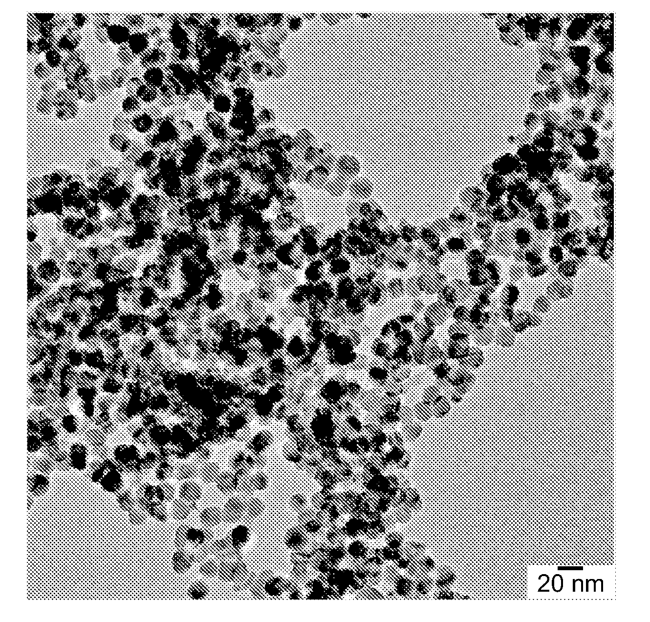
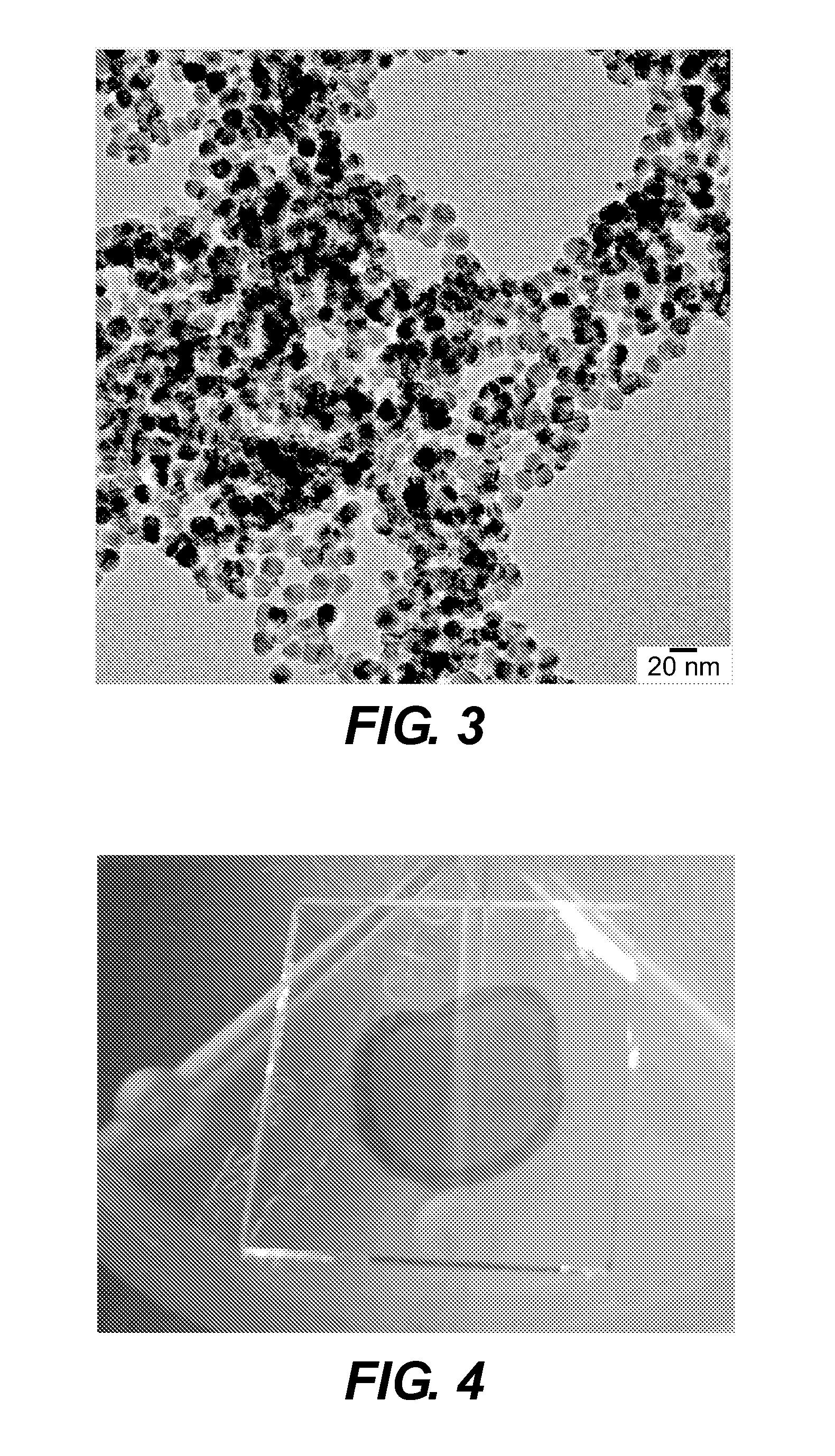
[0058]Polycrystalline films of nanocrystals having an aspect ratio less than 3:1 and a diameter greater than 10 nanometers were formed on glass substrates. The test system was CdSe. The cadmium precursor is cadmium acetate and the Se precursor is TOPSe. The coordinating solvent for the growth is a mixture of trioctylphosphine oxide (TOPO) hexadecylamine (HDA), and trioctylphosphine (TOP), which are degassed at 190° C., 100° C., and 190° C., respectively, for 60 minutes prior to their usage. In a small vial inside of a dry box, 0.23 g (1 mmol) of cadmium acetate is added to 3 ml TOP. After gently heating this mixture under constant spinning, the solution goes clear in 5-10 minutes. At the same time, a mixture of 6 ml of degassed TOPO and 3 ml of degassed HDA is placed in a three-neck flask and placed on a Schlenk line. At room temperature, the contents are subjected to three cycles of evacuation, and are then degassed at 100° C. for 30 minutes followed by argon refilling. Then 0.5 ml...


PUM


Abstract

A method of making a film of large II-VI nanocrystals, including: providing a mixture of column II, column VI chemical precursors, and coordinating solvents selected from amines, phosphines, phosphine oxides, esters, ethers, or combinations thereof by: injecting under heat a higher molar quantity of column II chemical precursor than column VI chemical precursor; and ii) increasing the ratio of column VI to column II chemical precursors during the course of the reaction while still heating the mixture until the molar ratio of column VI chemical precursor to column II chemical precursor is in a range of 1 to 10; heating the mixture to grow large nanocrystals functionalized with coordinating ligands; washing the grown nanocrystals to remove the unreacted precursors and excess coordinating solvents; and d) depositing the large II-VI nanocrystals on a substrate in order to form the film.

Description

CROSS-REFERENCE TO RELATED APPLICATIONS[0001]Reference is made to commonly-assigned, co-pending U.S. patent application Ser. No. ______ (Kodak Docket 95537US01) filed herewith, entitled “Semiconductor Nanocrystal Film” by Ren et al., the disclosure of which is incorporated herein.FIELD OF THE INVENTION[0002]The present invention relates to a method of making polycrystalline films composed of large-sized semiconductor nanocrystalsBACKGROUND OF THE INVENTION[0003]Charge transport layers containing n-type or p-type semiconductors can be used in making a variety of devices such as field effect transistors, bipolar transistors, p-n diodes, light emitting diodes (LEDs), lasers, sensors, solar cells and others. Most semiconductor devices in use today, both inorganic and organic, are in part or completely formed using expensive vacuum deposition processes. There are ongoing efforts to find a low cost manufacturing process, however, device performance has been inadequate for market needs. Th...

Claims


Application Information

Patent Timeline
Patent Type & Authority Applications(United States)
IPC IPC(8): H01L21/20
CPCC09K11/025H01L21/02628H01L21/02551C09K11/883
Inventor REN, XIAOFANKAHEN, KEITH B.
Owner EASTMAN KODAK CO
Why Eureka
Try Eureka