
Method for producing semiconductor device and semiconductor device

a technology of semiconductor devices and semiconductor devices, which is applied in the direction of solid-state devices, coatings, chemical vapor deposition coatings, etc., can solve the problems of raising the capacitance increase between the interconnects, difficult to reduce the specific dielectric constant sufficiently, so as to achieve the effect of easily and sufficiently lowering

Inactive Publication Date: 2011-08-18
RENESAS ELECTRONICS CORP
View PDF7 Cites 16 Cited by
  • Summary
  • Abstract
  • Description
  • Claims
  • Application Information

AI Technical Summary

Benefits of technology

[0014]According to the technique of International Application No. 2008 / 010591, a plurality of cyclosiloxane source materials are individually vaporized and thereafter mixed in a gaseous state and, in accordance therewith, the carrier gas mass flow increases. Due to increase in the carrier gas mass flow, the excited ion species in the plasma increase in number, whereby the side chain may be dissociated from the source material, or the cyclic skeleton structure may undergo ring-opening. This may decrease the amount of hydrocarbon contained in the layer or decrease the amount of introduced pores deriving from the cyclic skeleton structure, thereby also making it difficult to lower the specific dielectric constant sufficiently.
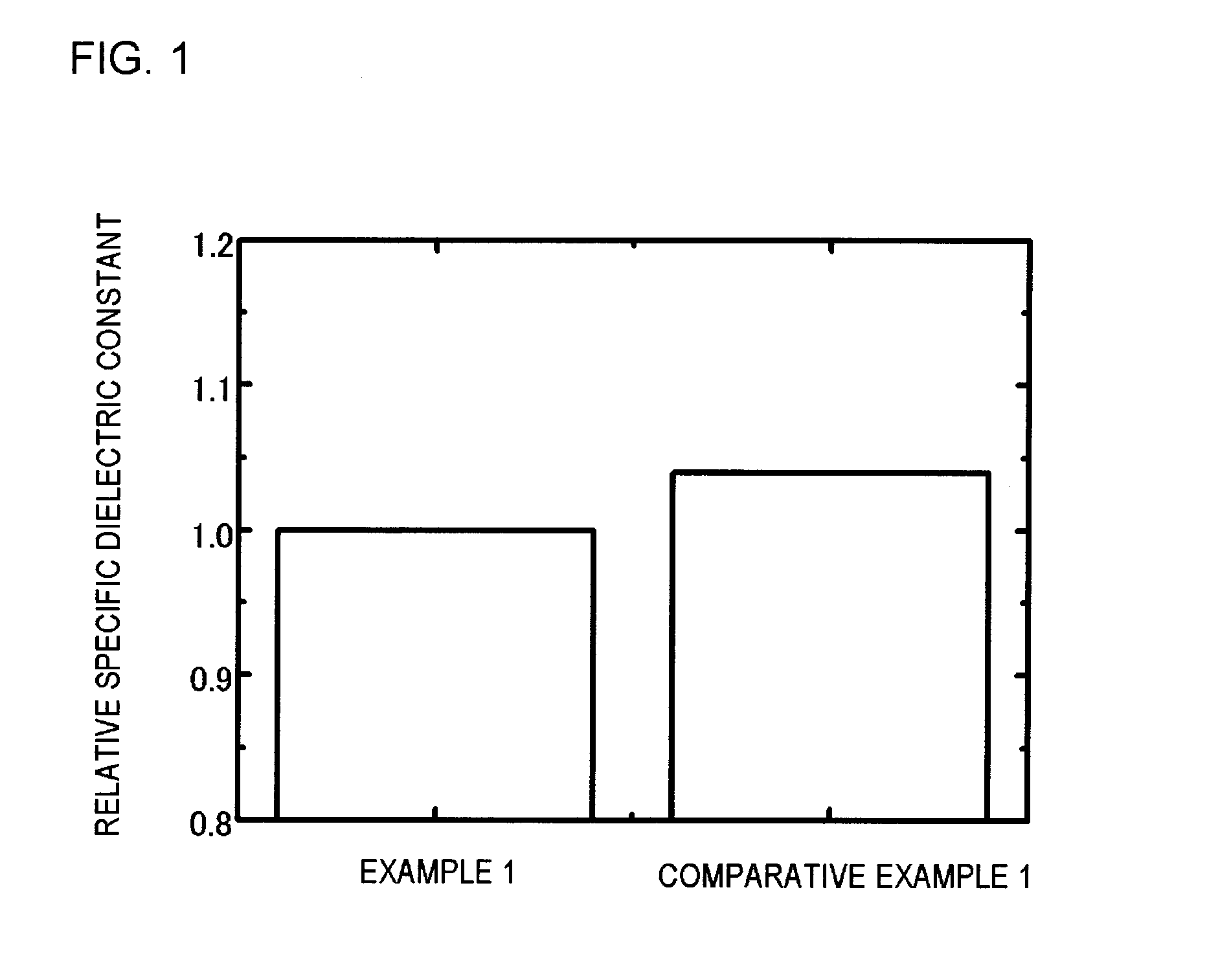
[0021]According to this production method, the electric dielectric constant of an insulating film can be easily lowered. Hereinafter, the reasons therefor will be described.
[0022]First, in this production method, by mixing and thereafter vaporizing two or more kinds of organic siloxane compound materials each having a cyclic SiO structure as a main skeleton and having different structures from each other or alternatively performing the mixing and vaporization simultaneously, the specific dielectric constant of the insulating film can be reduced. In other words, by incorporating the skeleton structure of a cyclic SiO compound into the insulating film, pores can be introduced into the insulating film, and the specific dielectric constant of the insulating film can be lowered.
[0026]Also, in forming an insulating film by using a plurality of liquid source materials, when the plural source materials are individually vaporized, the amount of carrier gas will be large. Generally, an inert gas is used as the carrier gas. However, since the carrier gas acts also as an excited gas in the plasma, decomposition such as dissociation of the side chain of the source material or ring-opening of the skeleton structure will proceed according as the amount of the carrier gas increases. As a result of this, it will be difficult to introduce fine pores into the insulating film, and also the amount of hydrocarbon that is taken into the insulating film decreases, thereby disadvantageously making it difficult to lower the specific dielectric constant of the insulating film. For this reason, instead of individually vaporizing the plural source materials, the plural source materials are mixed and thereafter vaporized, or the mixing and vaporization of the plural source materials are carried out simultaneously, whereby the carrier gas that transports the source materials can be reduced in amount. This can suppress the decomposition of the source materials, and can lower the dielectric constant of the insulating film.
[0030]According to the present invention, the specific dielectric constant of an insulating film can be easily and sufficiently lowered.

Problems solved by technology

In accordance with the miniaturization of the LSI in recent years, miniaturization of the interconnect dimension is also in progress, thereby raising a problem of increase in the capacitance between the interconnects.
According to the technique of International Application No. 2007 / 032261, the straight-chain material containing a part of the chemical structure constituting a organic cyclosiloxane material forms a Si—O—Si bond of high order, whereby an SiO2-oxide-layer-like part (having a k value of about 4) is formed in the layer, making it difficult to lower the specific dielectric constant sufficiently.
This may decrease the amount of hydrocarbon contained in the layer or decrease the amount of introduced pores deriving from the cyclic skeleton structure, thereby also making it difficult to lower the specific dielectric constant sufficiently.
However, this solvent is also involved in the polymerization reaction in the plasma, making it difficult to select an optimal material for realizing the decrease in the specific dielectric constant.
Thus, it has been difficult to lower the specific dielectric constant of an insulating film easily and sufficiently.
This method can realize reduction of the specific dielectric constant in a comparatively easy manner; however, it is difficult to miniaturize the pore size, and moreover, the pores are connected with each other because of the forming method, whereby large pores (open pores) larger than individual pores are formed, resulting in nonuniform layer density distribution.
As a result of this, it will be difficult to introduce fine pores into the insulating film, and also the amount of hydrocarbon that is taken into the insulating film decreases, thereby disadvantageously making it difficult to lower the specific dielectric constant of the insulating film.

Method used


Image

  • Method for producing semiconductor device and semiconductor device
  • Method for producing semiconductor device and semiconductor device
  • Method for producing semiconductor device and semiconductor device

Examples


first embodiment

[0075]In the present embodiment, an insulating film suitable as an insulating interlayer is formed by mixing at least two or more kinds of cyclic SiO compound materials and thereafter vaporizing the mixture in the same vaporizer and performing the plasma vapor growth method using this vaporized gas.

[0076]In the present embodiment, for example, the source materials all may be a cyclosiloxane represented by the chemical formula (1). As Rx and Ry in the chemical formula (1), it is preferable to use at least one straight-chain unsaturated hydrocarbon group having a carbon number of 2 to 4 or branched-chain saturated hydrocarbon group having a carbon number of 3 to 4. Each of the straight-chain unsaturated hydrocarbon groups and the branched-chain saturated hydrocarbon groups is, for example, one of vinyl, allyl, methyl, ethyl, propyl, isopropyl, butyl, and tertiary butyl group. Also, n is preferably set to be 3 or 4. Specifically, the cyclosiloxane represented by the chemical formula (1...

example 1

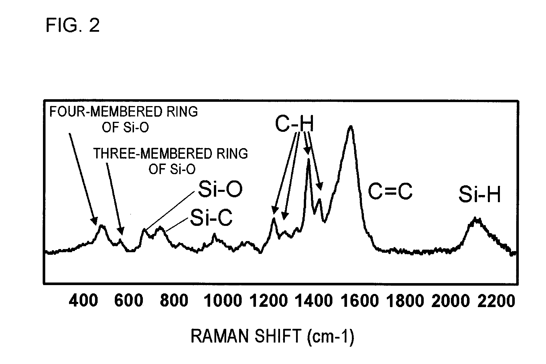
[0108]For forming an insulating film, first and second organic cyclosiloxanes respectively represented by the chemical formula (1) were used as source materials. Among these, as the first organic cyclosiloxane, a organic cyclosiloxane (2,4,6-triisopropyl-2,4,6-trivinylcyclotrisiloxane) in which R1 (Rx) is a vinyl group, R2 (Ry) is an isopropyl group, and n=3 was used. Also, as the second organic cyclosiloxane, a organic cyclosiloxane (2,4,6,8-tetravinyl-2,4,6,8-tetramethylcyclotetrasiloxane) in which R1 (Rx) is a vinyl group, R2 (Ry) is a methyl group, and n=4 was used. For forming the film, a plasma generating apparatus shown in FIG. 6 was used. Into the source material reservoir tank 226a, a liquid source material obtained by mixing these two kinds of source materials in a molar ratio of 4:3 (first organic cyclosiloxane being 4 relative to second organic cyclosiloxane being 3) was put and enclosed. As a carrier gas, He of 500 sccm was introduced into the vaporizer 216a via the gas...

example 2

[0113]When the steric hindrance effect of the side chains of the first and second organic cyclosiloxanes increases, it will be more effective for reduction of the dielectric constant. As source materials for forming an insulating film, first and second organic cyclosiloxanes were used. Among these, as the first organic cyclosiloxane, one having the same structure as the first organic cyclosiloxane of Example 1 was used (therefore, n=3). On the other hand, as the second organic cyclosiloxane, one being different from the first organic cyclosiloxane of Example 2 only in that the value of n was 4 (instead of 3) was used. Specifically, as the second organic cyclosiloxane to the first organic cyclosiloxane (2,4,6-triisopropyl-2,4,6-trivinylcyclotrisiloxane), a organic cyclosiloxane (2,4,6,8-tetravinyl-2,4,6,8-tetraisopropylcyclotetrasiloxane) in which R1 (Rx) is a vinyl group, R2 (Ry) is isopropyl, and n=4 was used. For forming the film, a plasma generating apparatus shown in FIG. 6 was ...


PUM

PropertyMeasurementUnit
Fractionaaaaaaaaaa
Angleaaaaaaaaaa
Temperatureaaaaaaaaaa

Abstract

In a method for producing a semiconductor device, two or more kinds of organic siloxane compound materials each having a cyclic SiO structure as a main skeleton and having different structures are mixed and thereafter vaporized. Alternatively, those two or more kinds of organic siloxane compound materials are mixed and vaporized simultaneously to produce a vaporized gas. Then, the vaporized gas is transported to a reaction furnace together with a carrier gas. Then, in the reaction furnace, a porous insulating layer is formed by the plasma CVD method or the plasma polymerization method using the vaporized gas.

Description

[0001]This application is based on Japanese Patent Application No. 2010-283111, the content of which is incorporated hereinto by reference.BACKGROUND OF THE INVENTION[0002]1. Technical Field[0003]The present invention relates to a method for producing a semiconductor device and to a semiconductor device.[0004]2. Related Art[0005]Conventionally, in silicon semiconductor integrated circuits (hereafter referred to as LSI), aluminum (Al) or Al alloy has been used as an electrically conductive material. Then, in accordance with a progress in miniaturization of the LSI, copper (Cu) has come to be used as an electrically conductive material in order to achieve reduction of interconnect resistance and higher reliability of the interconnect. Since Cu is easily diffused into a silicon oxide layer, an electrically conductive barrier metal layer for preventing diffusion of Cu is generally used on the side surface and on the bottom surface of the Cu interconnect, and an insulative barrier layer ...

Claims


Application Information

Patent Timeline
IPC IPC(8): H01L21/312
CPCC23C16/401H01L21/02126H01L21/7682H01L21/02216H01L21/02274H01L21/02203H01L21/76807H01L2221/1047H10B61/00
Inventor YAMAMOTOKAWAHARA, JUNSAKAGUCHI, TOMONORIHAYASHI, YOSHIHIRO
Owner RENESAS ELECTRONICS CORP
Learn More