Method of Group III Metal - Nitride Material Growth Using Metal Organic Vapor Phase Epitaxy

Inactive Publication Date: 2011-10-20
DETCHPROHM THEERADETCH +2
View PDF3 Cites 15 Cited by
  • Summary
  • Abstract
  • Description
  • Claims
  • Application Information

AI Technical Summary

Benefits of technology

[0027]In a fourth aspect of the present invention, the said seed layer can be easily destroyed by physical or chemical stress or processes, leading to the substrate removal from the as-grown film, leaving a free-standing epitaxial film suitable for e.g. wafer-bonding.
[0028]In a fifth aspect of the present inventi

Problems solved by technology

[06] Yet the most limiting factor for the nitride materials' practical usage is their high cost associated with the material fabrication itself.
At the same time, a polar growth orientation significantly limits the performance of semiconductor devices fabricated using such films.
In optoelectronics, in particular, the presence of high polarization fields leads to the effect known as Quantum Confined Stark Effect (QCSE) which causes spatial separation of electrons and holes inside a quantum well and therefore may reduce the efficiency of the light generation.
Although non-polar and semi-polar faces are usually considered as preferable for the optoelectronic applications, just preparing the corresponding crystal surfaces by, for example, bulk crystal polishing does not yet provide the material suitable for the device fabrication.
The limitation of this technique is the necessity of having bulk native substrate to prepare the initial layer stable enough to support the process of growth.
The said bulk substrate has to be obtained by some other method, which is often challenging and very expensive.
Until now, the availability of such bulk substrates is limited in quality and size, making this method unsuitable for the mass production.
Another important limitation is the uncontrolled growth of so-called twin crystals—two separate crystals that share some of the same crystal lattice points in

Method used


Image

  • Method of Group III Metal - Nitride Material Growth Using Metal Organic Vapor Phase Epitaxy
  • Method of Group III Metal - Nitride Material Growth Using Metal Organic Vapor Phase Epitaxy
  • Method of Group III Metal - Nitride Material Growth Using Metal Organic Vapor Phase Epitaxy

Examples


Embodiment Construction

E technique over the m-plane sapphire substrate.

[0034]FIG. 5 shows yet another lower-resolution DIC Microscopy image of the surface of semi-polar GaN deposited using conventional MOVPE technique over the m-plane sapphire substrate.

[0035]FIG. 6 shows a lower-resolution DIC Microscopy image of the surface of semi-polar GaN deposited using the technique of the present invention over the m-plane sapphire substrate.

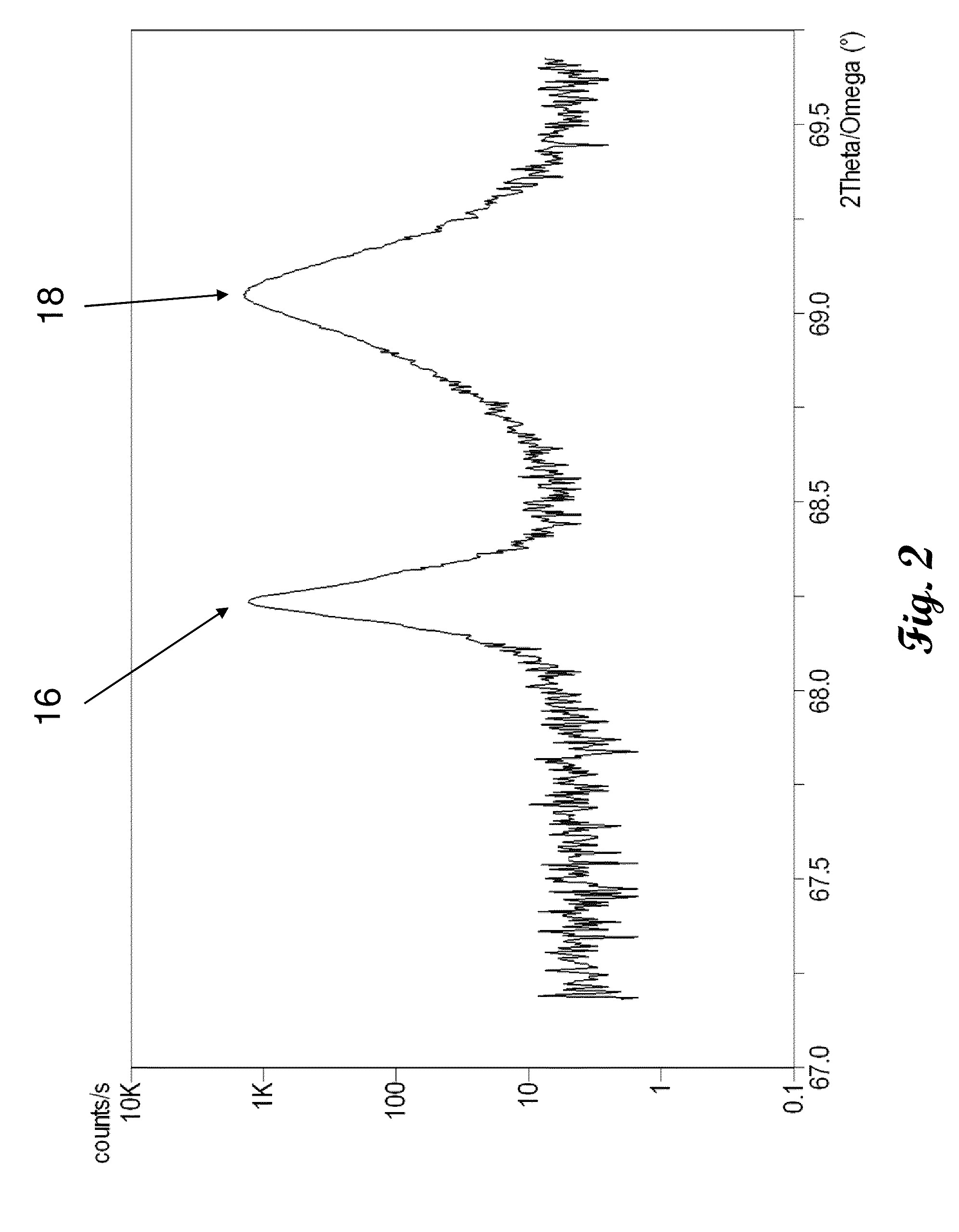
[0036]FIG. 7 presents the Transmission Electron Microscopy (TEM) high resolution image of the Substrate / Seed Layer / GaN layer deposited using the technique of the present invention.

[0037]FIG. 8 provides the insight to the face type validation of the grown GaN film by the method of Convergent Beam Electron Diffraction (CBED).

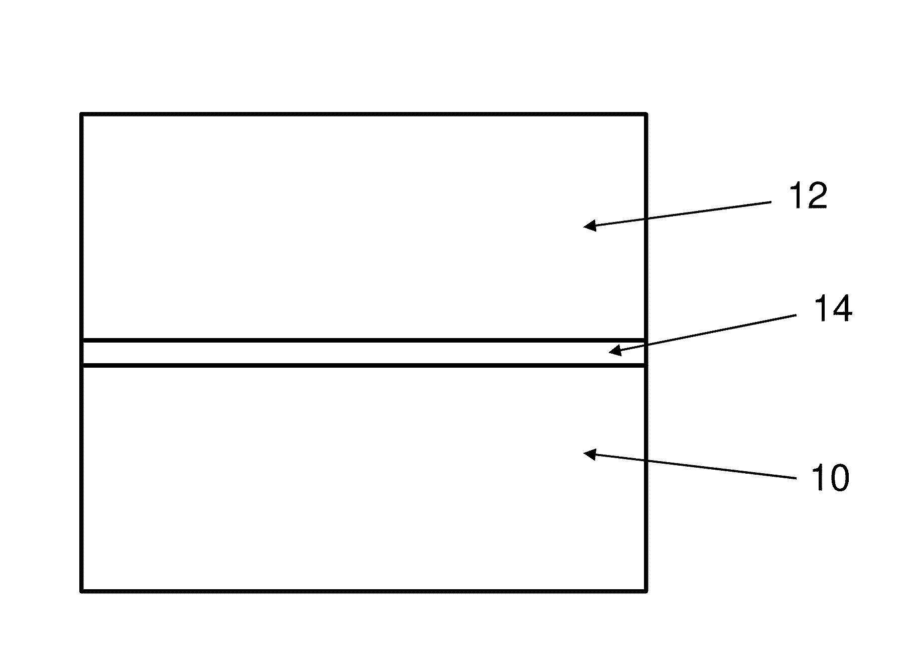
[0038]It is noted that FIG. 1 of the drawings accompanying the invention description is not to scale. The drawings are intended to depict only typical aspects of the invention, and therefore should not be considered as limiting the scope of the invention.

DET...


PUM

PropertyMeasurementUnit
Polarityaaaaaaaaaa
Flexibilityaaaaaaaaaa
Stress optical coefficientaaaaaaaaaa

Abstract

The non-polar or semi-polar Nitride film is grown using Metal Organic Vapor Phase Epitaxy over a substrate. The in-situ grown seed layer comprising Magnesium and Nitrogen is deposited prior to the Nitride film growth. The said seed layer enhances the crystal growth of the Nitride material and makes it suitable for electronics and optoelectronics applications. The use of non-polar and/or semi-polar epitaxial films of the Nitride materials allows avoiding the unwanted effects related to polarization fields and associated interface and surface charges, thus significantly improving the semiconductor device performance and efficiency. In addition, the said seed layer is also easily destroyable by physical or chemical stress, including the ability to dissolve in water or acid, which makes the substrate removal process available and easy. The substrate removal provides the possibility to achieve exceptional thermal conductivity and application flexibility, such as additional contact formation, electromagnetic radiation extraction, packaging or other purposes suggested or discovered by the skilled artisan.

Description

CROSS-REFERENCE TO RELATED APPLICATION[0001]This application claims the benefit of Provisional Patent Application Ser. No. 61 / 325,609, filed on Apr. 19, 2010 by present inventors.FEDERALLY SPONSORED RESEARCH[0002]Not ApplicableSEQUENCE LISTING OR PROGRAM[0003]Not ApplicableFIELD OF THE DISCLOSURE[0004]Aspects of the invention relate to the compound semiconductor material growth technique over a substrate, and in particular, to the Metal Organic Vapor Phase Epitaxy (MOVPE) of Boron Nitride, Aluminum Nitride, Gallium Nitride, Indium Nitride, and their combinative compounds in the crystalline direction, other than Ga-polar <0001> direction, over commercially available, cost-effective large area substrates.BACKGROUND OF THE DISCLOSURE[0005]Gallium Nitride and related alloys (Indium Nitride, Aluminum Nitride and their ternary and quaternary alloys, referred here as Nitride materials) are emerging materials for many applications in semiconductor industry, for electronics and especia...

Claims


Application Information

Patent Timeline
IPC IPC(8): H01L29/20B32B38/10C30B25/02
CPCC30B25/02C30B29/403H01L21/0242Y10T156/11H01L21/02439H01L21/0254H01L21/0262H01L21/02433
Inventor DETCHPROHM, THEERADETCHZHU, MINGWEIWETZEL, CHRISTIAN
Owner DETCHPROHM THEERADETCH
Why Eureka
Try Eureka