Ion source cleaning in semiconductor processing systems

a technology of ion source and processing system, which is applied in the direction of vacuum evaporation coating, cleaning of hollow articles, coatings, etc., can solve the problems of affecting the performance of the ion source, affecting the ion source region, and affecting the ion source lifetime, so as to prolong the lifetime of the ion implant system and improve the performance. , the effect of improving the performan

Inactive Publication Date: 2011-10-27
ENTEGRIS INC
View PDF4 Cites 28 Cited by
  • Summary
  • Abstract
  • Description
  • Claims
  • Application Information

AI Technical Summary

Benefits of technology

[0033]A further aspect of the invention relates to a method of maintaining a predetermined electrical resistance of a filament of an ion source in an arc chamber, comprising contacting the filament with a reagent effective to deposit material on the filament or to etch material from the filament depending on temperature in the arc chamber, and controlling temperature in the arc chamber to effect deposition or etching of material at the filament, so as to maintain said predetermined electrical resistance.
[0034]In another aspect, the invention relates to a method of cleaning an ion implantation system or one or more components thereof, to remove ionization-related deposits therefrom, comprising contacting the ion implantation system or one or more components thereof with BrF3 under conditions in which said BrF3 is chemically reactive with the deposits to effect at le

Problems solved by technology

In the ideal case, all feedstock molecules would be ionized and extracted, but in reality a certain amount of feedstock decomposition occurs, which results in the deposition on and contamination of the ion source region.
The residue can form on low voltage insulators in the ion source, causing electrical short circuits which can interrupt the arc required to produce thermionic electrons.
This phenomenon is generally known as “source glitching,” and it is a major contributor to ion beam instability, and may eventually cause premature failure of the source.
The residue also forms on the high voltage components of the ion implanter, such as the source insulator or the surfaces of the extraction electrodes, causing energetic high voltage sparking.
Such sparks are another contributor to beam instability, and the energy released by these sparks can damage sensitive electronic components, leading to increased equipment failures and poor MTBF.
Another common problem can occur with antimony (Sb+) implant using Sb2O3 as the solid doping material, which can be exacerbated by running boron (B) even after only a few hours of Sb+ implantation.
The boron beam current can significantly deteriorate with performance and lifetime of ion source significantly compromised.
The cause of this degradation in performance is due to the excessive Sb deposited on the source chamber and its components.
Failure of the ion source significantly reduces implanter productivity as throughput is reduced due to more frequent preventive maintenance or less beam current.
But some of the deposits (e.g. solid phosphorus) are pyrophoric and can ignite during the manual maintenance operations.
Not only is this a fire hazard, but toxic compounds also can be liberated.
In another cause of ion source failure, various materials

Method used


Image

  • Ion source cleaning in semiconductor processing systems
  • Ion source cleaning in semiconductor processing systems
  • Ion source cleaning in semiconductor processing systems

Examples


example 1

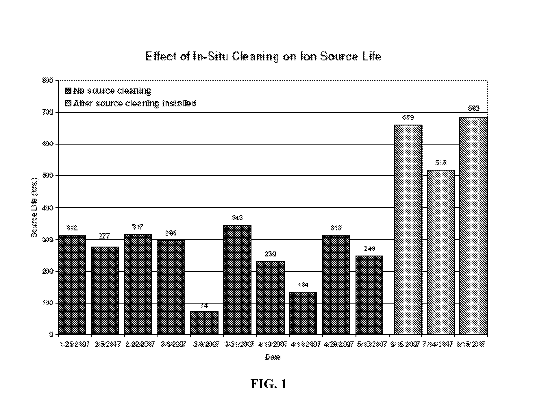
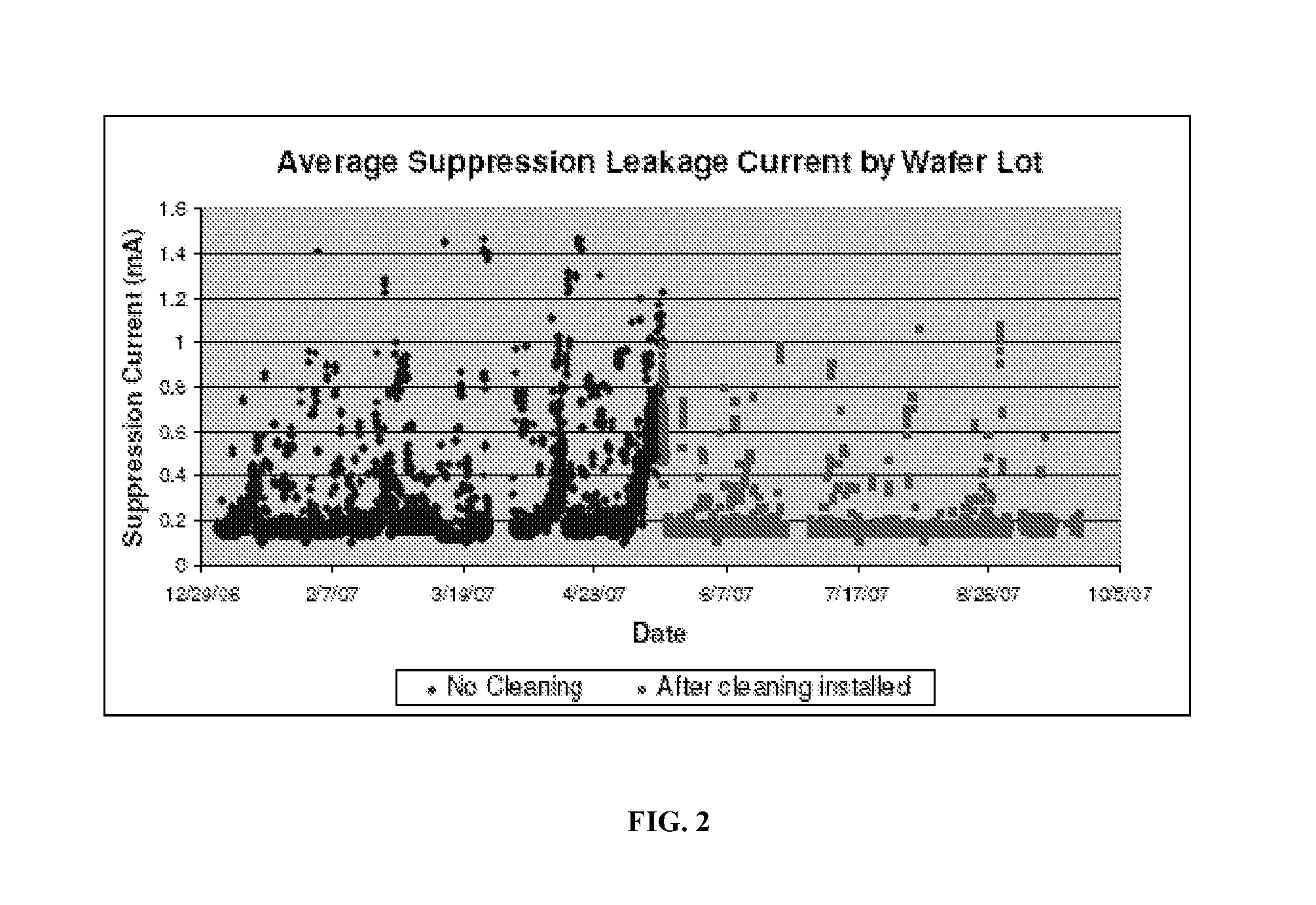
[0142]This example shows the improvement in ion source lifetime and implanter utilization that is achievable by use of a chemical cleaning agent to remove deposits. Preferably, the deposits are removed at regular intervals to prevent buildup of contaminant flakes and conductive films in the implanter.

[0143]In-situ cleaning was carried out by introducing XeF2 at regular intervals from a supply vessel thereof positioned in the gas box of the ion implanter, with XeF2 cleaning vapor introduced into the ion source for 10-15 minutes twice a day. A high current implanter was utilized for testing to assess flow dynamics of the cleaning reagent. XeF2 cleaning properties were determined and it was verified that the cleaning agent had no adverse effect on the implanter's beamline components. The cleaning process using the XeF2 reagent then was qualified for use with a medium current implanter apparatus.

[0144]FIG. 1 is a graph of compiled source lifetime data from such medium current implanter,...

example 2

[0158]This example demonstrates the control of filament growth, in an ion source of an illustrative ion implanter system.

[0159]FIG. 5A is a graph showing the effects of XeF2 flow and arc power variation, with respect to increased filament current and weight. The graph shows filament weight in grams, as a function of elapsed time, in hours, of operation of the implanter system. The upper line in the graph represented operation at an XeF2 flow of 2.2 standard cubic centimeters per minute (sccm) and arc power of 100 volts / 0.05 amps, for which a filament weight gain of 319 milligrams / hour was determined after 3 hours of operation. The lower line in the graph reflected an XeF2 flow of 0.5 seem and arc power of 40 volts / 0.05 amps, which produced a filament weight gain of 63 milligrams / hour for the 3 hour duration of operation.

[0160]FIG. 5B is a graph showing the effects of XeF2 flow and arc power variation, with respect to filament current. The graph shows filament current in amperes, as ...


PUM

PropertyMeasurementUnit
Flow rateaaaaaaaaaa
Massaaaaaaaaaa
Massaaaaaaaaaa

Abstract

Cleaning of an ion implantation system or components thereof, utilizing a reactive cleaning reagent enabling growth/etching of the filament in an ion source of the arc chamber, by appropriate control of temperature in the arc chamber to effect the desired filament growth or alternative filament etching. Also described is the use of reactive gases such as XeFx, WFx, AsFx, PFx and TaFx, wherein x has a stoichioimetrically appropriate value or range of values, for cleaning regions of ion implanters, or components of implanters, in in situ or ex situ cleaning arrangements, under ambient temperature, elevated temperature or plasma conditions. Among specific reactive cleaning agents, BrF3 is described as useful for cleaning ion implant systems or component(s) thereof, in in situ or ex situ cleaning arrangements. Also described is a method of cleaning the forelines of an ion implant system for at least partial removal of ionization-related deposit from said forelines, comprising contacting said forelines with a cleaning gas wherein said cleaning gas is chemically reactive with said deposit. Also described is a method of improving the performance and extending the lifetime of an ion implant system, comprising contacting the cathode with a gas mixture.

Description

FIELD OF THE INVENTION[0001]The present invention relates to monitoring, control and cleaning of material deposition on components of semiconductor processing systems, in particular to ion implantation systems.DESCRIPTION OF THE RELATED ART[0002]Ion implantation is used in integrated circuit fabrication to accurately introduce controlled amounts of dopant impurities into semiconductor wafers and is a crucial process in microelectronic / semiconductor manufacturing. In such implantation systems, an ion source ionizes a desired dopant element gas and the ions are extracted from the source in the form of an ion beam of desired energy. Extraction is achieved by applying a high voltage across suitably shaped extraction electrodes, which incorporate apertures for passage of the extracted beam. The ion beam is then directed at the surface of the workpiece, such as a semiconductor wafer, in order to implant the workpiece with the dopant element. The ions of the beam penetrate the surface of t...

Claims


Application Information

Patent Timeline
IPC IPC(8): B08B7/00H01L21/265B08B5/00
CPCC23C14/48C23C14/54C23C14/564H01J37/08H01J2237/22H01J37/18H01J37/3171H01J2237/082H01J37/16H01L21/02041H01L21/265H01L21/3065
Inventor SWEENEY, JOSEPH D.YEDAVE, SHARAD N.BYL, OLEGKAIM, ROBERTELDRIDGE, DAVIDSERGI, STEVENFENG, LINBISHOP, STEVEN E.OLANDER, W. KARLTANG, YING
Owner ENTEGRIS INC
Why Eureka
Try Eureka