Organic solvent development or multiple development pattern-forming method using electron beams or EUV rays
a technology of organic solvent and pattern-forming method, which is applied in the direction of photomechanical treatment originals, photomechanical instruments, etc., can solve the problems of high sensitivity, high resolution, and insatiable pattern form and residual film rate in super fine processing regions, and achieve high sensitivity, improve the performance of fine processing of semiconductor devices, and improve the effect of fine processing
- Summary
- Abstract
- Description
- Claims
- Application Information
AI Technical Summary
Benefits of technology
Problems solved by technology
Method used
Image
Examples
synthesis example 1
Synthesis of Resin (A1-1)
[0400]In nitrogen current, 20 g of cyclohexanone is put in a three-neck flask and heated at 80° C. (solvent 1). M-1, M-2, M-3 and M-4 shown below are dissolved in cyclohexanone at a molar rate of 40 / 10 / 40 / 10 to prepare a monomer solution (200 g) of 22% by mass. Further, a solution obtained by adding 6 mol % of initiator V-601 (manufactured by Wako Pure Chemical Industries) to the monomer and dissolving is dripped into solvent 1 over 6 hours. After termination of dripping, the reaction solution is further reacted at 80° C. for 2 hours. The reaction solution is allowed to be cooled, and then poured into a mixed solution comprising 1,400 ml of hexane and 600 ml of ethyl acetate. The powder precipitated is collected by filtration and dried to obtain 37 g of resin (A1-1). From GPC, weight average molecular weight (Mw: polystyrene-equivalent) of resin (A1-1) is 10,000, and polydispersity (Mw / Mn) is 1.6.
[0401]Resins (A1-2) to (A1-8) are synthesized in the similar m...
synthesis example 2
Synthesis of Resin (A2-1)
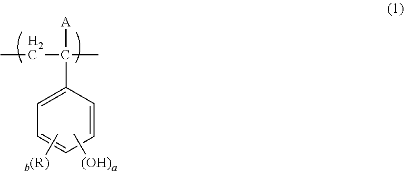
[0402]In nitrogen current, 4.66 parts by mass of 1-methoxy-2-propanol is heated at 80° C. A mixed solution comprising 7.0 parts by mass of 4-hydroxystyrene, 3.0 parts by mass of monomer (M-5), 18.6 parts by mass of 1-methoxy-2-propanol, and 1.36 parts by mass of dimethyl-2,2′-azobisisobutyrate (V-601, manufactured by Wako Pure Chemical Industries) is dripped into the above liquid over two hours while stirring the liquid. After termination of dripping, the reaction solution is stirred at 80° C. for further 4 hours. The reaction solution is allowed to be cooled, and then the reaction product is re-precipitated with a large amount of hexane / ethyl acetate and vacuum dried to obtain 5.9 parts by mass of resin (A2-1) of the invention.
[0403]From GPC, weight average molecular weight (Mw: polystyrene-equivalent) of resin (A2-1) is Mw=15,100, and polydispersity (Mw / Mn) is 1.40.
[0404]Resins (A2-2) to (A2-6) are synthesized in the similar method.
2.1 EB Exposure
examples 1 to 18
(1) Preparation of Coating Solutions of Actinic Ray-Sensitive or Radiation-Sensitive Resin Compositions, and Application Thereof
[0405]The solution of the actinic ray-sensitive or radiation-sensitive resin composition is obtained by precisely filtering the coating solution composition having the composition shown in Table 1 through a membrane filter having a pore size of 0.1 μm. In Table 1, the ratio in the case of using two or more components is a mass ratio.
[0406]The solution of the actinic ray-sensitive or radiation-sensitive resin composition is applied on a 6-inch Si wafer having been subjected to HMDS treatment in advance with a spin coater Mark 8 (manufactured by Tokyo Electron Limited), dried on a hot plate at 100° C. for 60 seconds, and a resist film having a thickness of 0.08 μm is obtained.
(2) Evaluation of EB Exposure
[0407]Pattern irradiation is performed on the resist film obtained in the above (1) with an electron beam imaging apparatus (HL750, accelerating voltage: 50 ...
PUM
 Abstract
Description
Claims
Application Information


