Method of manufacturing gas barrier film and organic photoelectric conversion element
a technology of gas barrier film and conversion element, which is applied in the direction of final product manufacturing, sustainable manufacturing/processing, liquid/solution decomposition chemical coating, etc., can solve the problems of many defects in the film, deterioration of the gas barrier property as a whole of the formed film, and low productivity of these methods, etc., to achieve excellent surface lubricity and bending resistance, high gas barrier property, and high product quality
- Summary
- Abstract
- Description
- Claims
- Application Information
AI Technical Summary
Benefits of technology
Problems solved by technology
Method used
Image
Examples
example 1
Preparation of Gas Barrier Film
[Preparation of Gas Barrier Film 1]
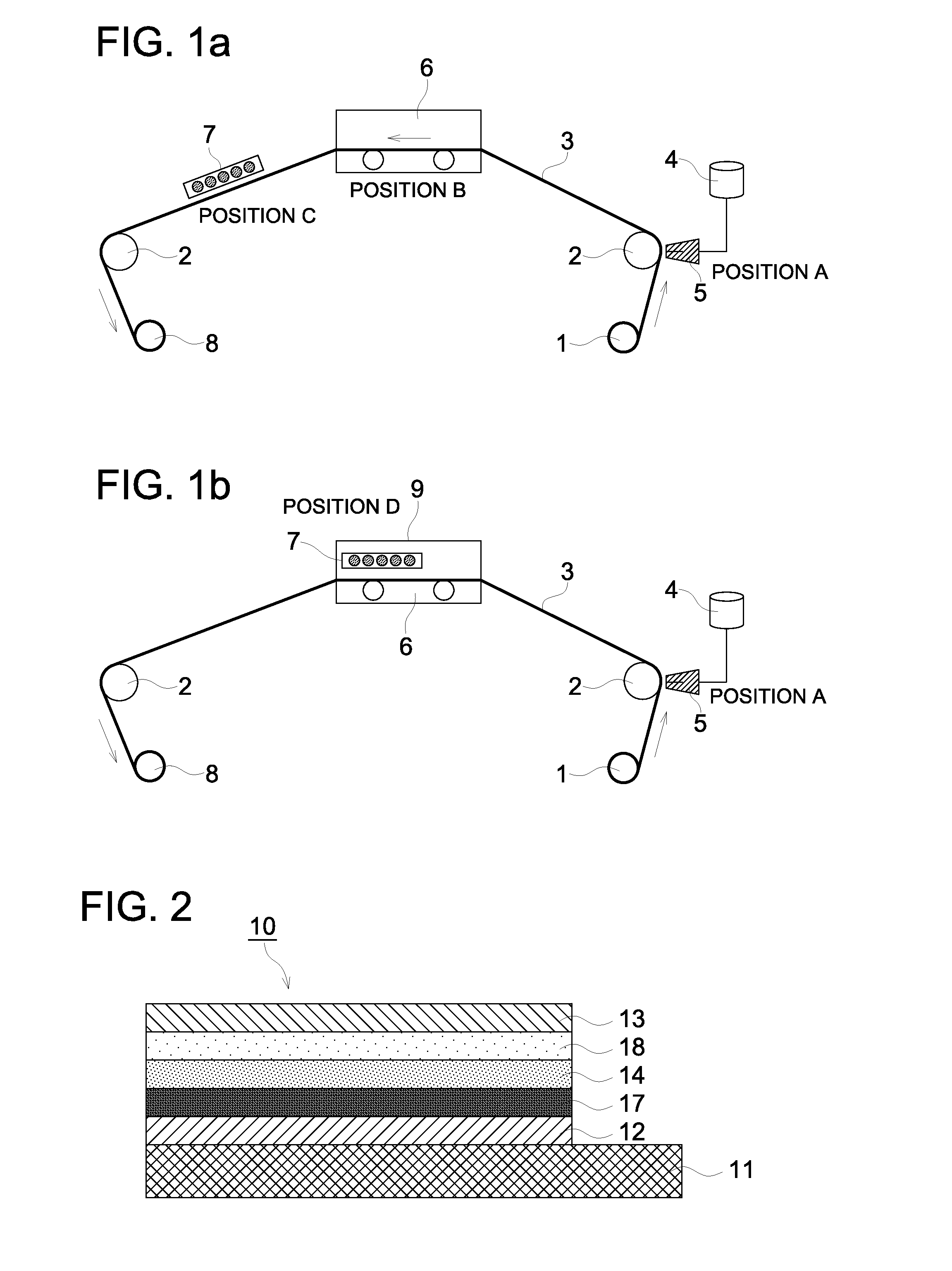
[0239]Gas barrier film 1 was prepared according to the manufacture line of the gas barrier film shown in FIG. 1a, in which a drying process and a modification process are separated.
Preparation of Substrate
[0240]As a thermoplastic resin substrate, employed was a polyethylene terephthalate film having a thickness of 125 μm, both surfaces of which had been subjected to an easy adhesive treatment (super-low heat shrinkage PET Q83, produced by Teijin Dupont Films Japan Ltd.).
Preparation of Bleedout Preventing Layer
[0241]On one surface of the above substrate, a UV curable organic / inorganic hybrid hard coat material OPSTAR Z7535 produced by JSR Corp. was applied using a wire bar so that the thickness after dried was 4 μm, followed by conducting a hardening treatment under a hardening condition: 1.0 J / cm2, in air, and using a high-pressure mercury lamp, and a drying condition: 80° C. for 3 minutes. Thus, a bleedout preven...
example 2
Preparation of Organic Photoelectric Conversion Element
[0285]Employing each of the gas barrier films prepared in Example 1, Organic photoelectric conversion elements 1 to 12 were prepared.
[0286]On each of the gas barrier films, a first electrode was formed by patterning an indium-tin oxide (ITO) transparent conductive film accumulated to a thickness of 150 nm (of which sheet resistance was 10Ω / □) to a width of 2 mm via a commonly used photolithographic technique and a wet etching technique. The patterned first electrode was washed via sequential steps of ultrasonic washing using a surfactant and ultra pure water and ultrasonic washing using ultra pure water, followed by drying under a nitrogen flow, and, finally, cleaned via ultraviolet / ozone cleaning.
[0287]On this transparent substrate, an electroconductive polymer Baytron P4083 (produced by Starck Vitec, Co.) was applied so that the thickness was 30 nm, and then dried. Subsequently, the layer was subjected to a heat treatment at...
PUM
| Property | Measurement | Unit |
|---|---|---|
| Temperature | aaaaa | aaaaa |
| Temperature | aaaaa | aaaaa |
| Percent by mass | aaaaa | aaaaa |
Abstract
Description
Claims
Application Information
 - R&D
- Intellectual Property
- Life Sciences
- Materials
- Tech Scout
- Unparalleled Data Quality
- Higher Quality Content
- 60% Fewer Hallucinations
Browse by: Latest US Patents, China's latest patents, Technical Efficacy Thesaurus, Application Domain, Technology Topic, Popular Technical Reports.
© 2025 PatSnap. All rights reserved.Legal|Privacy policy|Modern Slavery Act Transparency Statement|Sitemap|About US| Contact US: help@patsnap.com


