Ambipolar silicon nanowire field effect transistor

a technology of field effect transistor and silicon nanowire, which is applied in the direction of nanotechnology, electrical equipment, semiconductor devices, etc., can solve the problems of precise alignment of the two gates at the sides, independent doping, and disadvantages of technology

Active Publication Date: 2013-11-28
ECOLE POLYTECHNIQUE FEDERALE DE LAUSANNE (EPFL)
View PDF12 Cites 54 Cited by
  • Summary
  • Abstract
  • Description
  • Claims
  • Application Information

AI Technical Summary

Benefits of technology

[0027]In a ninth aspect the invention provides use of a silicon nanowire (SiNW) field effect transistor device with a double independent gate structure, the silicon nanowire field effect transistor comprising a first gate used to build up an electric field potential to modulate regions of a SiNW channel affected by a presence of a Schottky barrier interface, that comprises an interface region between the metal-to-semiconductor contact; and a depleted region in the semiconductor whose depletion is consequence of the presence of the Schottky contact. The silicon nanowire field effect transistor further comprises a second gate structure utilized to produce an electric field potential, which modulates further regions of the semiconducting channel not affected by the presence of a Schottky barrier interface, namely a portion of the channel, as a basic tile for fabrication of a sea-of-gates topology.
[0028]In a tenth aspect the invention provides use of a silicon nanowire (SiNW) field effect transistor device with a double ...

Problems solved by technology

However, the structures described in [2] have the only purpose of achieving threshold tuning but at the same time present technological disadvantages such as the precise alignment of the two gates at the sides of the channel, and...

Method used


Image

  • Ambipolar silicon nanowire field effect transistor
  • Ambipolar silicon nanowire field effect transistor
  • Ambipolar silicon nanowire field effect transistor

Examples


1st example

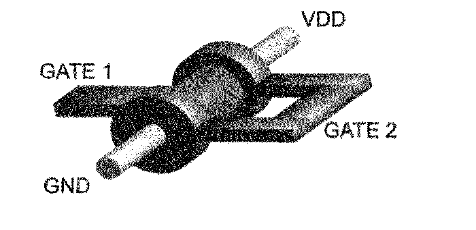
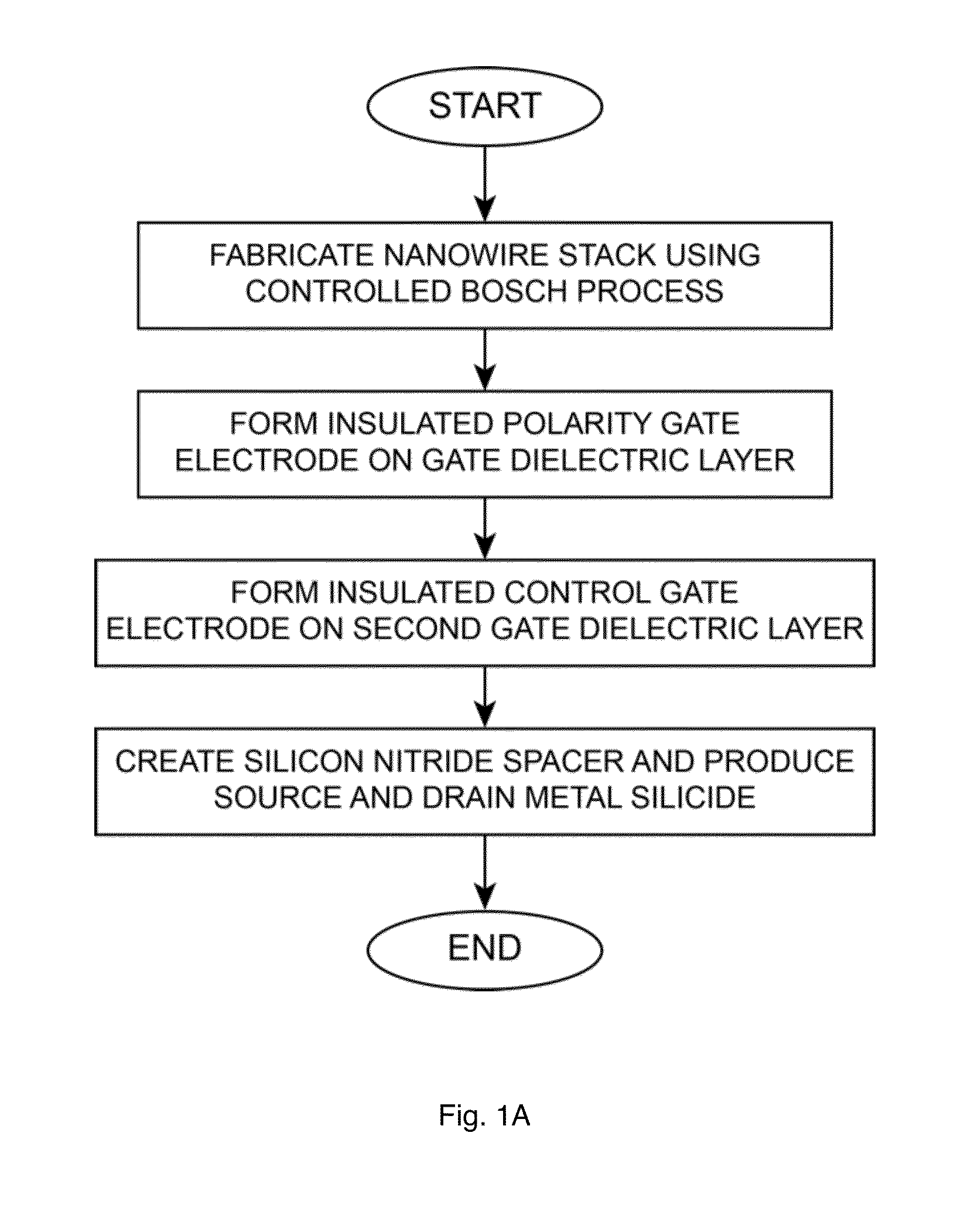
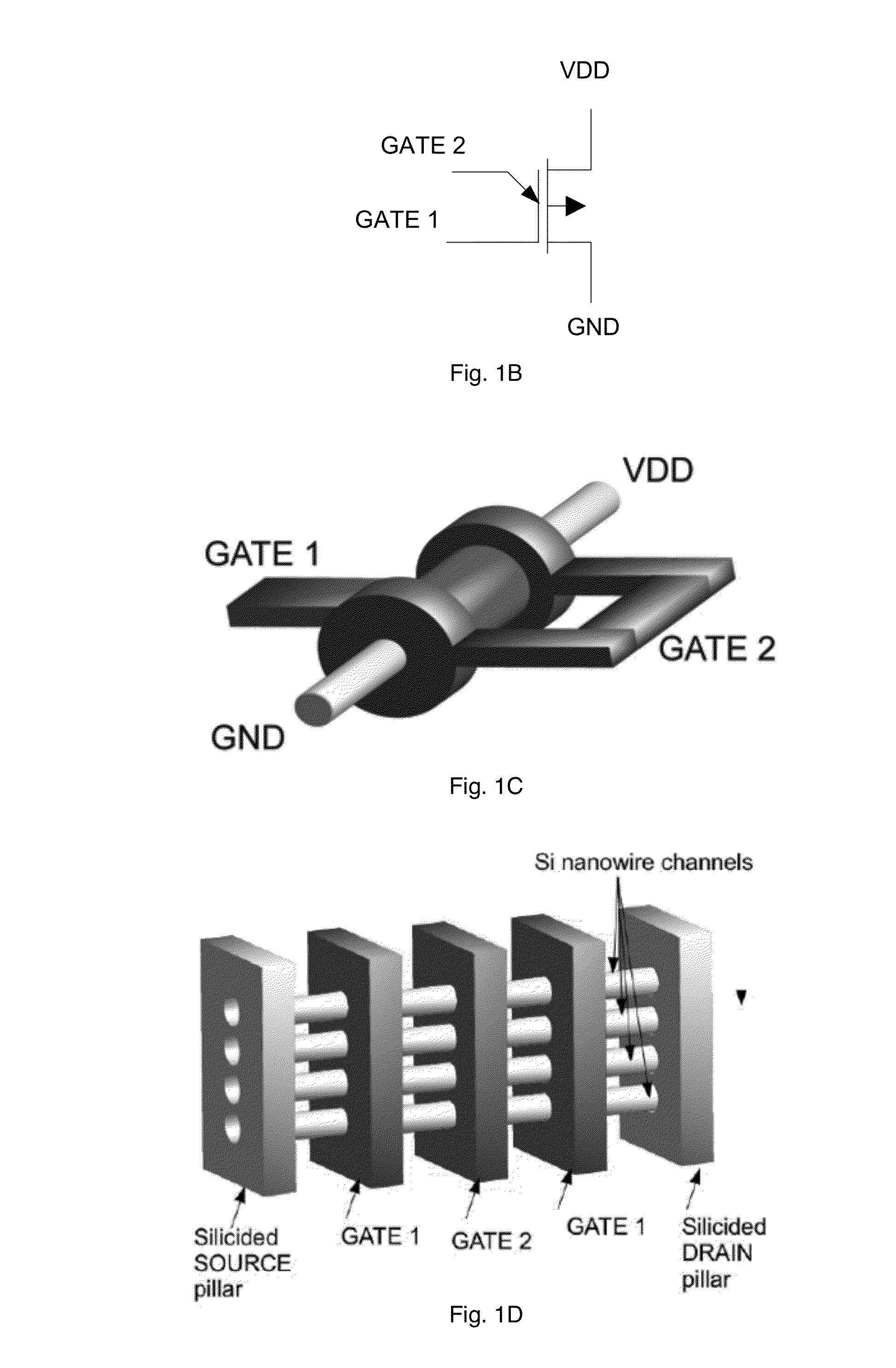
[0071]In a 1st example, the main steps of the device fabrication procedure are listed in FIG. 1A. Generally, the process includes creating a transistor channel, which can be composed of a vertical stack of a variable number of horizontal semiconducting nanowires, a parallel array of vertical stacks of horizontal nanowires, a fin-like structure (from which a FinFET transistor would be obtained) or a graphene ribbon. We will use the nanowire stack further on in this description as an example. FIG. 2B shows a cross section of the nanowire stack, with two pillar-like structures sustaining the nanowires, while FIG. 2A shows the top view of such stack.

[0072]After the channel structure is fabricated, a first gate insulator covering the channel section of the transistor is created. This gate insulator can be produced by direct oxidation of the transistor channel, or by deposition of various high-k dielectric materials.

[0073]A 1st gate electrode is deposited over the 1st gate insulator, and ...

2nd example

[0077]In a 2nd example, a single Si nanowire with Double Independent Gates is fabricated (see Top View of FIG. 3A). A low doping p-type (NA˜1015 atoms / cm2) SOI wafer with 1.5 μm device layer is spin coated. The photoresist is then patterned in 1.5 μm wide lines (see FIG. 3B) and used as mask for a next isotropic Si etching. A Si plasma etching recipe is tuned to form a triangular 75 nm wide Si nanowire lying on top of the buried oxide (BOX) layer (FIG. 3C). Then a 30 nm thick gate oxidation and a 150 nm polysilicon layer are deposited with a low-pressure chemical vapor deposition (LPCVD) method to form a main gate with 7.5 μm length (gate 1, FIG. 3D). 300 nm LPCVD low temperature oxide (LTO) is used to isolate the main gate. A second 500 nm polysilicon layer is then deposited. Then a thick photoresist is spun over the wafer and planarized using a chemical mechanical polishing procedure. This method leaves a protective polymer layer that is used to etch a second polysilicon gate self...

3rd example

[0078]In a 3rd example, vertical Si nanowires with Double Independent Gate All-Around are fabricated (see FIG. 4A). The Si nanowires are vertically etched in parallel on 10 SOI wafers after having patterned a SiO2 hard mask by lithography (FIG. 4B and FIG. 4C). The Si nanowire are then freestanding and anchored at the bottom where a Si layer is still left for subsequent processing (FIG. 4C). Then a SiO2 or a Si3N4 layer is deposited all-around by LPCVD method on 9 and 1 SOI wafer, respectively. Then SiO2 / Si3N4 spacers are formed by vertical plasma etching in a dry etching tool (FIG. 4D). At this stage, the Si nanowires are surrounded by a SiO2 or a Si3N4 dielectric, while the planar layer on top of the Buried Oxide and the top section of the Si nanowires reveal a non-passivated Si surface or with a native Si oxide thinner than 10 angstroms. Then another lithography defines the bottom layer that is etched in order to isolate the Si nanowires (FIG. 4E). Subsequently, a Ni metal laye...


PUM


Abstract

This invention describes a novel electronic device consisting of one—or more—vertically stacked gate-all-around silicon nanowire field effect transistor (SNWFET) with two independent gate electrodes. One of the two gate electrodes, acting on the central section of the transistor channel, controls on/off behavior of the channel. The second gate, acting on the regions in proximity to the source and the drain of the transistor, defines the polarity of the devices, i.e. p or n type. The electric field of the second gate acts either at the interface of the nanowire-to-source/drain region or anywhere in close proximity to the depleted region of the SiNW body, modulating the bending of the Schottky barriers at the contacts, eventually screening one type of charge carrier to pass through the channel of the transistor. This is achieved by controlling the majority carriers passing through the transistor channel by regulating the Schottky barrier thicknesses at the source and drain contacts.

Description

FIELD OF INVENTION[0001]The present invention relates to silicon nanowire field effects transistors (SNWFETs) and more precisely to new SNWFET architectures and processes for manufacturing such architectures.BACKGROUND[0002]Bulk CMOS technologies are predicted to face crucial technological challenges in the next decade. At the same time, novel devices such as Carbon Nanotube Field Effect Transistors (CNTFETs) and Silicon Nanowire Field Effect Transistors (SNWFETs), which do not suffer from the same constraints, are expected to play a primary role as devices in future ultra-large scale integration technologies.[0003]The interest in these devices is motivated not only by their small size, but also their superior characteristics, such as quasi-ballistic transport, steep sub-threshold slopes and one-dimensional channel geometry. Channel geometry, specifically, plays a major role in the current efforts towards miniaturization of devices, with transistor manufacturers currently moving fro...

Claims


Application Information

Patent Timeline
IPC IPC(8): H01L29/775H01L29/66
CPCH01L29/775H01L29/66439B82Y10/00H01L29/0673H01L29/42356H01L29/42392H01L29/7839H01L29/78642H01L29/78696
Inventor DE MICHELI, GIOVANNILEBLEBICI, YUSUFDE MARCHI, MICHELESACCHETTO, DAVIDE
Owner ECOLE POLYTECHNIQUE FEDERALE DE LAUSANNE (EPFL)
Why Eureka
Try Eureka