Monolithic integrated lattice mismatched crystal template and preparation method thereof
Inactive Publication Date: 2015-01-22
SHANGHAI INST OF MICROSYSTEM & INFORMATION TECH CHINESE ACAD OF SCI
View PDF4 Cites 8 Cited by
Summary
Abstract
Description
Claims
Application Information
AI Technical Summary
This helps you quickly interpret patents by identifying the three key elements:
Problems solved by technology
Method used
Benefits of technology
Benefits of technology
The present invention is providing a method for preparing a monolithic integrated lattice mismatched crystal template using low-viscosity material. This method has advantages of simple preparation, achieving various lattice constant material combinations on one substrate, and low dislocation density, high crystal quality compared to prior art methods. This can solve the problems of complicated process, limited material combinations, and low crystal quality in existing heteroepitaxial growth technology.
Problems solved by technology
For example: silicon (Si) crystal is the most common and inexpensive microelectronic material; but it cannot be used as luminescent material due to that Si is an indirect-band-gap material.
However, due to various crystals have their own lattice constant, only a very limited number of compounds (unless lattice matched) can achieve epitaxial growth on a specific commercial substrate with several tens of nanometers without generating a large number of defects (the defects include dislocations, stacking faults, interface and surface undulation, etc.).
The lack of substrates with arbitrary lattice constant results in that people cannot try all possible combinations of materials, thus being forced to limit the design of device structure on the existing substrates.
However, the major problem is still the lack of a suitable substrate.
Once again, the bottleneck to improve the performance of such devices is still high-quality substrate or template with the required lattice constants.
In the U.S. Pat. No. 5,294,808 (invention title: Pseudomorphic and dislocation free heteroepitaxial structures) belonging to Lo as the inventor, the compliant substrate template consists of a very thin membrane structure or platform shaped structure, but such method needs complicated preparation process and is hard to achieve large size.
However, all abovementioned approaches need to perform external process to achieve a compliant growth condition, and cannot be repeated in the same epitaxial growth process.
Such method has good effect for specific materials, but more material combinations are hard to obtain.
To sum up, the above methods have its disadvantages to solve the lattice mismatch issue.
Method used
Image
Click on the blue label to locate the original text in one second.
Reading with bidirectional positioning of images and text.
Examples
first embodiment
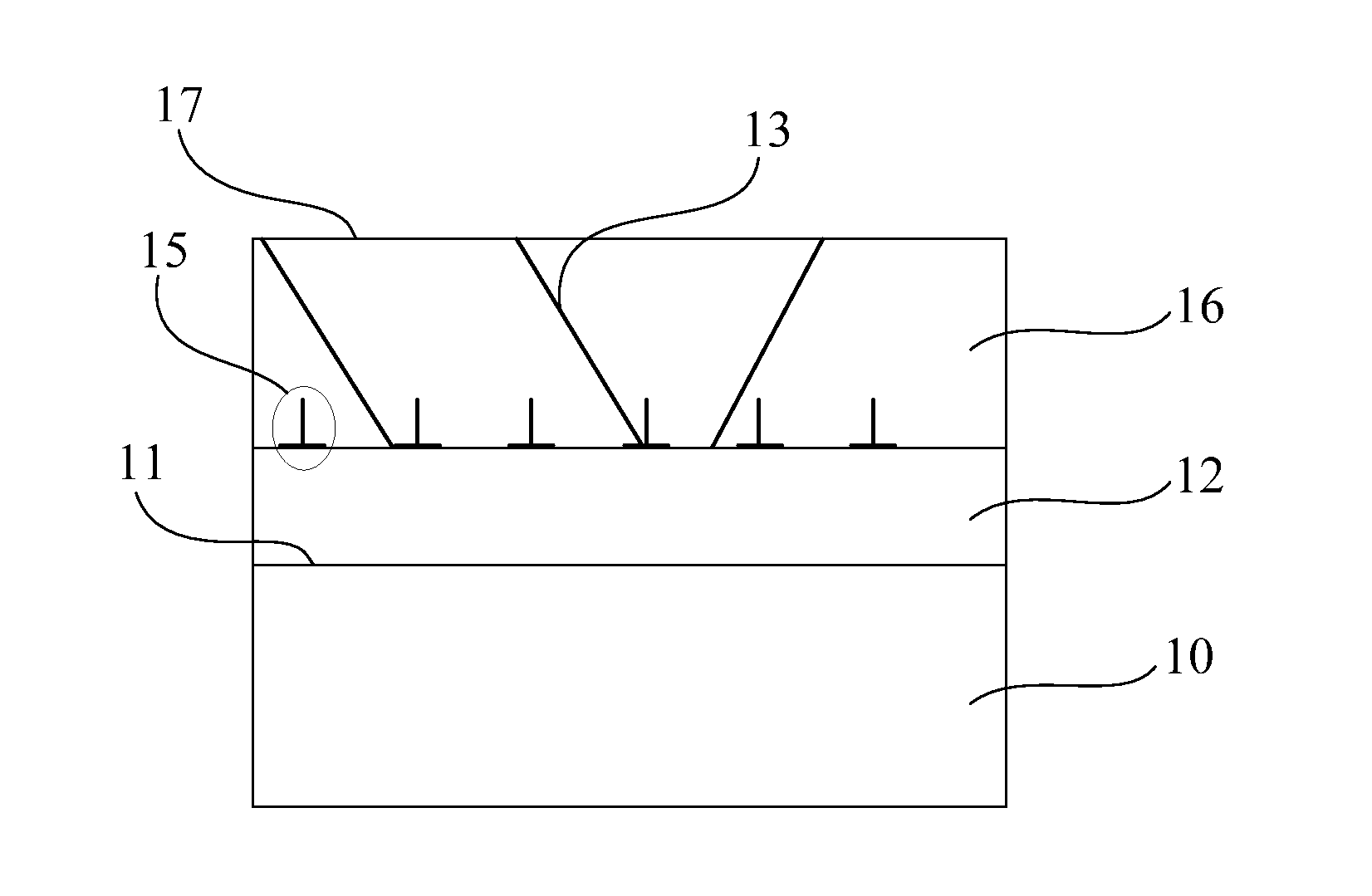
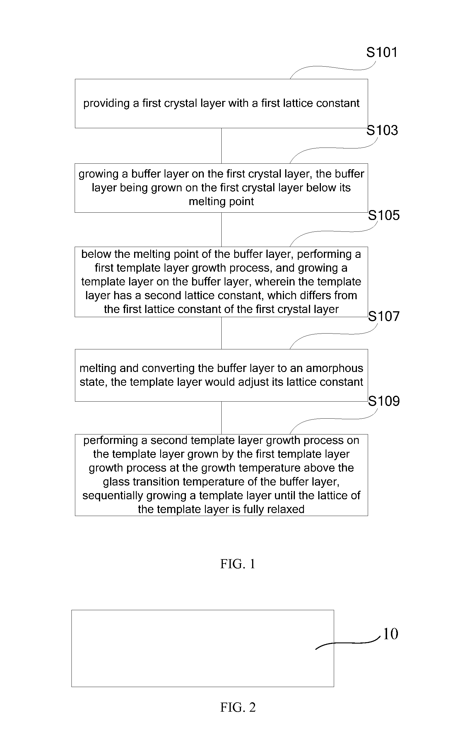
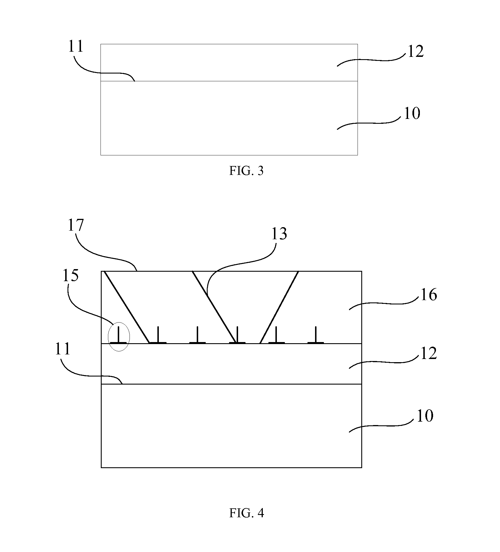
[0041]FIG. 1 is a flow diagram of the first embodiment of the preparation method for a lattice mismatched crystal template of the present invention. As shown in FIG. 1, the preparation method includes the following steps:
[0042]Step S101, providing a first crystal layer with a first lattice constant;
[0043]Step S103, growing a buffer layer on the first crystal layer, the buffer layer being grown on the first crystal layer at a temperature below the melting point of the buffer layer;
[0044]Step S105, below the melting point of the buffer layer, performing a first template layer growth process, and growing a template layer on the buffer layer, wherein the template layer has a second lattice constant, which differs from the first lattice constant of the first crystal layer;
[0045]Step S107, melting and converting the buffer layer to an amorphous state, the template layer would adjust its lattice constant.
[0046]Step S109, performing a second template layer growth process on the template lay...
second embodiment
[0063]FIG. 7 is a flow diagram of the second embodiment of the preparation method for a lattice mismatched crystal template of the present invention. It should be particularly stated that, since some process steps in the second embodiment is the same or similar with that in the first embodiment, the description in the second embodiment would focus on the part distinguished from that in the first embodiment.
[0064]As shown in FIG. 7, the preparation method includes the following steps:
[0065]Step S201, providing a first crystal layer with a first lattice constant;
[0066]Step S203, growing a buffer layer on the first crystal layer, the buffer layer being grown on the first crystal layer at a temperature below its melting point;
[0067]Step S205, below the melting point of the buffer layer, growing a second crystal layer on the buffer layer;
[0068]Step S207, below the melting point of the buffer layer, performing a first template layer growth process, and growing a template layer on the seco...
embodiment 1
In0.3Ga0.7As Template on a GaAs Substrate
[0094]Obviously, ternary In0.3Ga0.7As template is applicable for the design of 1.55 μm InGaAs / InAlAs tele-communication lasers with optimal conduction band mismatch and high thermal stability. Since unstrained bulk material of In0.3Ga0.7As has a band gap of 1 eV, it is suitable to be used as one of the junctions to form a multi junction solar cell with high efficiency.
[0095]According to the invention, the steps for growing In0.3Ga0.7As by molecular beamepitaxy (MBE) technique are followed:
[0096]A GaAs buffer layer is grown on a GaAs substrate to smooth the surface, at the growth temperature of 580° C.
[0097]Through interfacial misfit dislocation array (IMF) method, AlSb or GaSb with a thickness of 0.5 micron (μm) is grown at the growth temperature of 500° C. to 520° C. By forming misfit dislocation array at the interface, the IMF method may achieve in effective strain relaxation, and ensure a low threading dislocation density (optimum value l...
PUM
Property
Measurement
Unit
Temperature
aaaaa
aaaaa
Lattice constant
aaaaa
aaaaa
Thickness
aaaaa
aaaaa
Abstract
The present invention provides a monolithic integrated lattice mismatched crystal template and a preparation method thereof by using low-viscosity material, the preparation method for the crystal template includes: providing a first crystal layer with a first lattice constant; growing a buffer layer on the first crystal layer; below the melting point of the buffer layer, growing a second crystal layer and a template layer by sequentially performing the growth process of a second crystal layer and the growth process of a first template layer on the buffer layer, or growing a template layer by directly performing a first template layer growth process on the buffer layer; melting and converting the buffer layer to an amorphous state, performing a second template layer growth process on the template layer grown by the first template layer growth process at the growth temperature above the glass transition temperature of the buffer layer, sequentially growing a template layer until the lattice of the template layer is fully relaxed. Compared to the prior art, the invention has advantages of simple preparation, achieving in various lattice constant material combinations on one substrate and low dislocation density, high crystal quality.
Description
BACKGROUND OF THE PRESENT INVENTION[0001]1. Field of Invention[0002]The present invention relates to a manufacturing filed of semiconductor devices, and provides a monolithic integrated lattice mismatched crystal template and a preparation method thereof for large, low cost substrates by using low-viscosity material.[0003]2. Description of Related Arts[0004]1. The world today deduces a major turning point for optoelectronic devices transforming from discrete part to integrate part. Due to various kinds of restrictions and constraints based on the material, structure and process, optoelectronic integration needs to solve a series of essential basic scientific issues to make great strides.[0005]The ideal way to realize optoelectronic integration is growing different kinds of material systems on one material substrate (namely material compatibility), and integrating superior performance of all kinds of materials. For example: silicon (Si) crystal is the most common and inexpensive micr...
Claims
Application Information
Patent Timeline
Application Date:The date an application was filed.
Publication Date:The date a patent or application was officially published.
First Publication Date:The earliest publication date of a patent with the same application number.
Issue Date:Publication date of the patent grant document.
PCT Entry Date:The Entry date of PCT National Phase.
Estimated Expiry Date:The statutory expiry date of a patent right according to the Patent Law, and it is the longest term of protection that the patent right can achieve without the termination of the patent right due to other reasons(Term extension factor has been taken into account ).
Invalid Date:Actual expiry date is based on effective date or publication date of legal transaction data of invalid patent.

