

Thin film transistor
- Summary
- Abstract
- Description
- Claims
- Application Information
AI Technical Summary
Benefits of technology
Problems solved by technology
Method used
Image

Examples
experimental example 1
ESL TFT
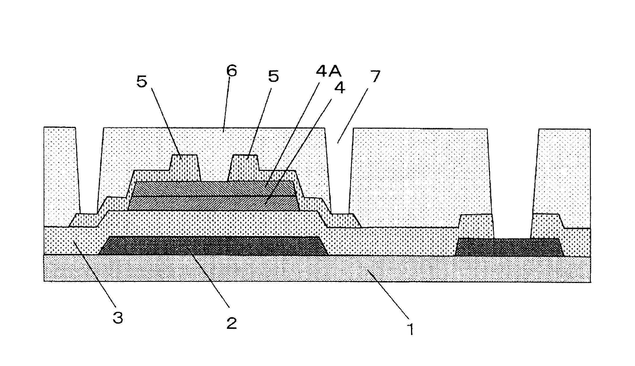
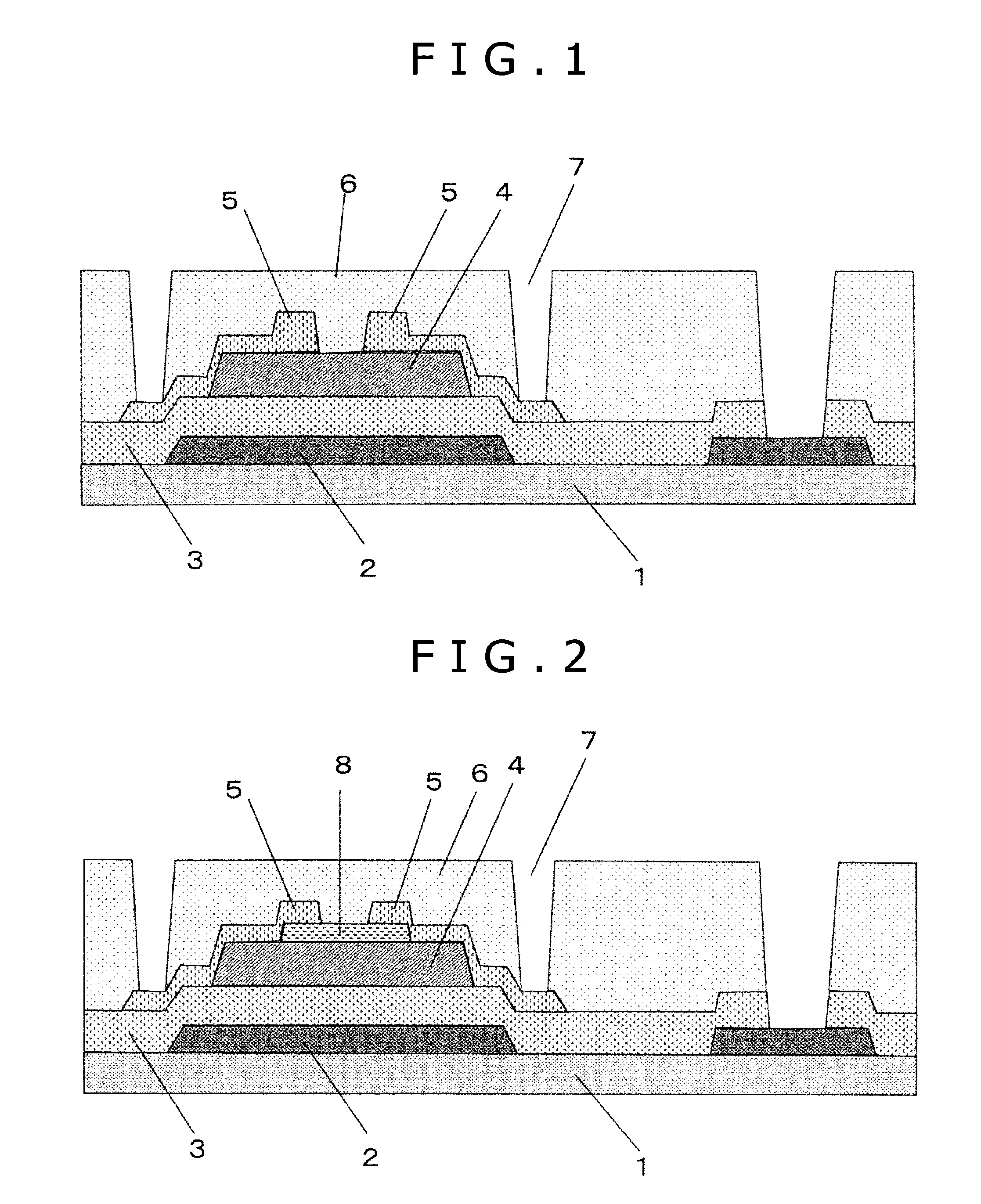
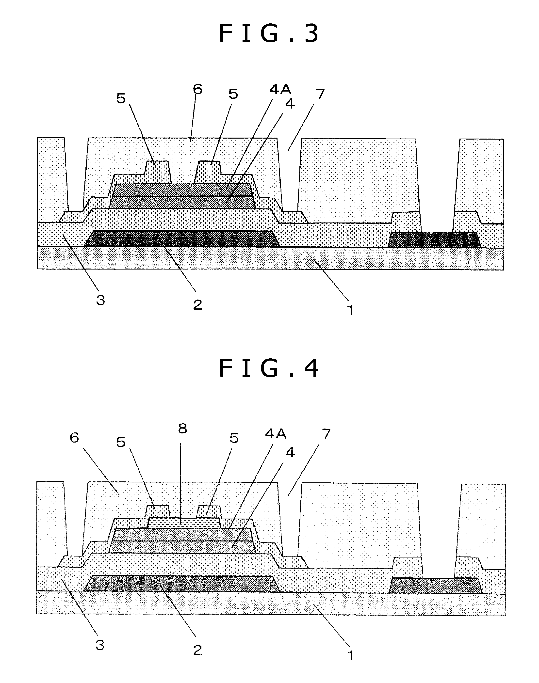
[0149]In this experimental example, ESL TFTs (FIG. 4) including oxide semiconductor layers of various types were produced and were evaluated on characteristics.
[0150]First oxide semiconductor layers were formed in this experimental example using two different IGZTOs, i.e., IGZTO “A” and IGZTO “B” given in Table 1. These IGZTOs are both examples having metal element ratios meeting the conditions specified in the present invention.
[0151]Second oxide semiconductor layers were formed in this experimental examples using a total of eleven (11) different IGZTOs, i.e., IGZTOs “a” to “k” given in Table 2. Among them, the IGZTOs “a” to “c” and “k” are examples having metal element ratios meeting the conditions specified in the present invention, and the IGZTOs “d” to “j” are examples having metal element ratios not meeting one or more of the conditions specified in the present invention.
[0152]Initially, a molybdenum (Mo) thin film having a thickness of 100 nm as a gate electrode 2 and ...
experimental example 2
BCE TFT
[0224]In this experimental example, the etching rate of each oxide semiconductor layer by a resist stripper was measured to evaluate resistance to resist stripper. For simplified measurement, the oxide semiconductor layer was deposited not to have a multilayer structure, but to have a single layer structure of a first oxide semiconductor layer alone. The etching rate was measured in a manner as follows.
[0225]Two different IGZTOs “A” and “B” in Table 6 were used to form the first oxide semiconductor layer. These are oxides meeting conditions in metal element ratios specified in the present invention and are the same as the IGZTOs “A” and “B” in Table 1. For comparison, an IGZO “C” (including no Sn, having an atomic ratio of In:Ga:Zn of 1:1:1) as given in Table 6 was used to form the first oxide semiconductor layer.
TABLE 6First oxide semiconductorGa / (In + Sn / (In + Ga / (In + Ga +Ga +SymbolInGaZnSnGa)Zn + Sn)Zn + Sn)A174033100.700.400.15B171747190.500.320.19C33.333.333.300.500.500...
experimental example 3
BCE TFT
[0243]In this experimental example, BCE TFTs including various oxide semiconductor layers were produced and evaluated on characteristics. This experimental example employed the oxides “A” to “C” in Table 7 to form the first oxide semiconductor layer and the oxide IGTO “a” in Table 2 to form the second oxide semiconductor. The source-drain electrodes were etched herein using a wet etchant.
[0244]Initially, a molybdenum (Mo) thin film having a thickness of 100 nm as a gate electrode 2, and a SiO2 film having a thickness of 250 nm as a gate insulator film 3 were sequentially deposited on or over a glass substrate 1 (Corning's EAGLE XG, 100 mm in diameter by 0.7 mm in thickness). The gate electrode 2 was deposited by direct-current sputtering using a pure molybdenum (Mo) sputtering target at a deposition temperature of room temperature, a deposition power of 300 W, with a carrier gas of Ar, and at a gas pressure of 2 mTorr. The gate insulator film 3 was deposited by plasma CVD, wi...
PUM
 Abstract
Description
Claims
Application Information