Composition and method for making picocrystalline artificial carbon atoms

a technology of artificial carbon atoms and composition, which is applied in the direction of crystal growth process, non-metal conductors, group 3/13 element organic compounds, etc., can solve the problems of affecting practical applications, affecting the practical application of nonlinear nuclear configurations, and inability to combine these materials with monocrystalline silicon, etc., to achieve short range and long-range order

Inactive Publication Date: 2016-12-01
SEMINUCLEAR INC
View PDF1 Cites 13 Cited by
  • Summary
  • Abstract
  • Description
  • Claims
  • Application Information

AI Technical Summary

Benefits of technology

[0012]These materials are also unique in that they contain picocrystalline quantum dots that form artificial atoms. The picocrystalline quantum dots (in the form of boron icosahedra with a nearly-symmetrical nuclear configuration) can replace corner silicon atoms in a structure that demonstrates both short range and long-range order as determined by x-ray diffraction of actual samples. The picocrystalline oxysilaboranes tend to form a borane solid with a continuous network quite similar to that of monocrystalline silicon, albeit a continuous random network in which certain silicon atoms are selectively replaced by picocrystalline quantum dots comprising boron icosahedra with symmetrical nuclear configuration. By varying oxygen content and the presence or absence of a significant impurity such as gold, unique electrical devices can be constructed that improve upon and are compatible with current semiconductor technology.

Problems solved by technology

220-235: All nonlinear nuclear configurations are unsuitable for an orbitally-degenerate electronic state.
While the study of graphene has advanced the general understanding of quantum electrodynamics in condensed matter physics, inherent limitations in its structure and, indeed, the structure of the allotropes of carbon, hinder practical applications.
Chief among such limitations is an inability to combine these materials with monocrystalline silicon, on which the electronics industry has been built.

Method used


Image

  • Composition and method for making picocrystalline artificial carbon atoms
  • Composition and method for making picocrystalline artificial carbon atoms
  • Composition and method for making picocrystalline artificial carbon atoms

Examples


example 1

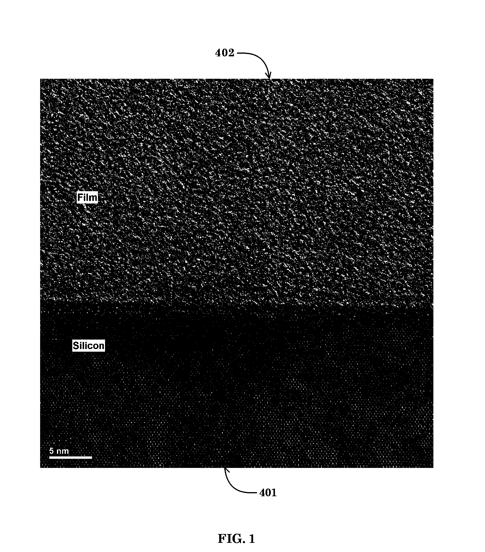
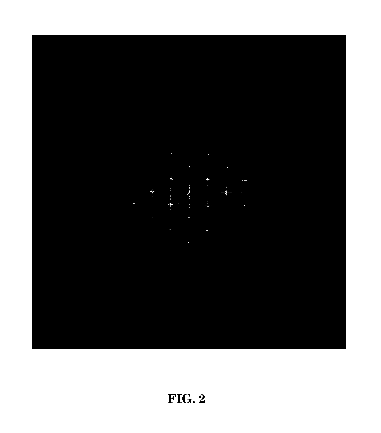
[0079]FIG. 1 shows a micrograph obtained by high-resolution transmission electron microscopy (HRTEM) of a picocrystalline borane solid 402 deposited on a monocrystalline (001) silicon substrate 401. The interfacial layer 403 is due to the specific conditions of its deposition. An HRTEM fast Fourier transform (FFT) image of the monocrystalline silicon substrate 401 is shown in FIG. 2. A similar FFT image of the picocrystalline borane solid 402 is shown in FIG. 3. Whereas the FFT image of the silicon substrate 401 in FIG. 2 is characteristic of a monocrystalline (001) silicon lattice with a long-range periodic translational order, the FFT image of the picocrystalline solid 402 within FIG. 3 exhibits a short-range order that is not characteristic of either a monocrystalline lattice or an amorphous solid. The various types of order will now be further defined.

[0080]To illustrate the short-range order of the picocrystalline borane solid 402, the HRTEM diffraction intensity of the monocry...

example 2

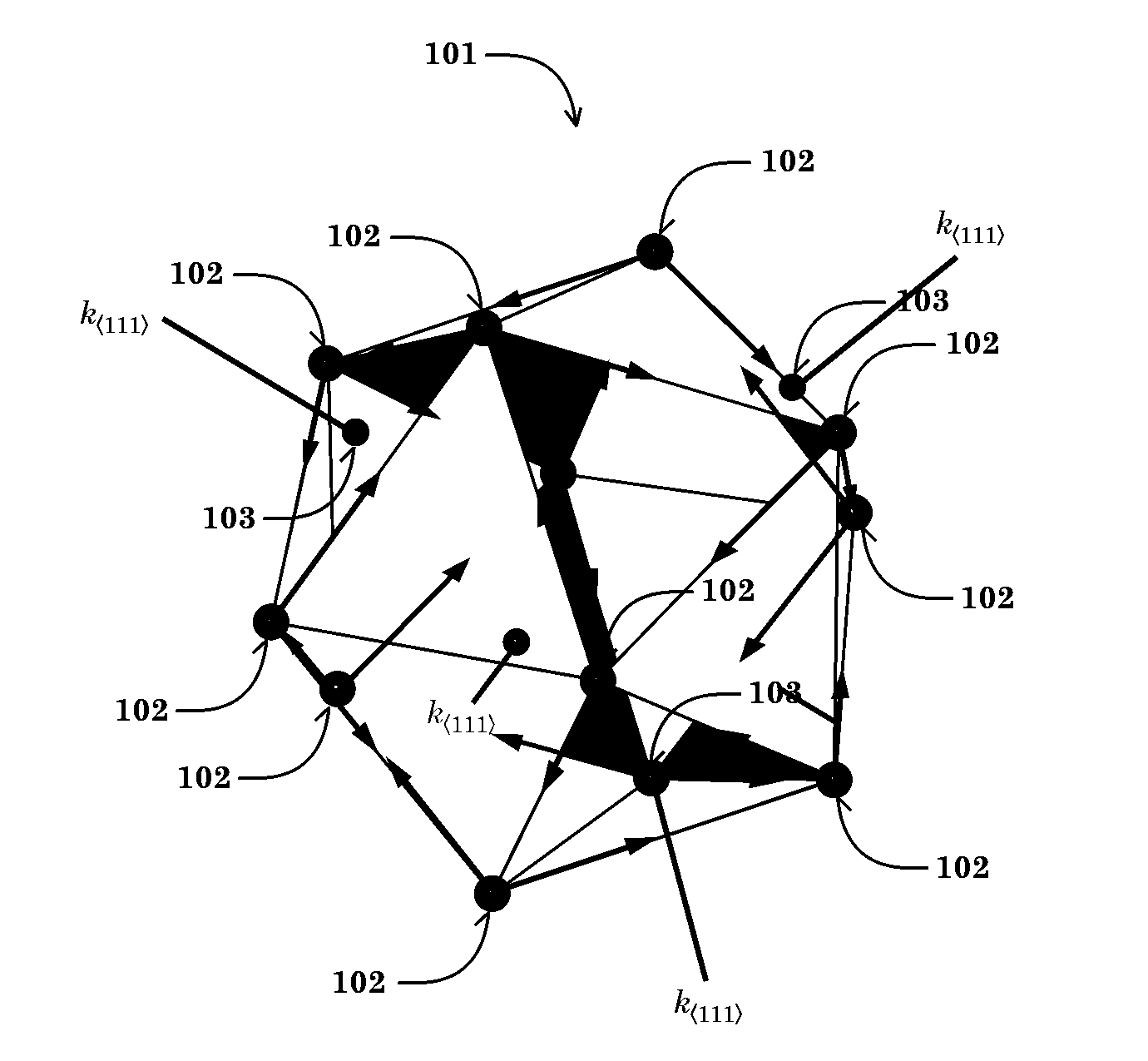
[0096]A diamond-like picocrystalline silaborane unit cell 300 is constructed by replacing each silicon vertex atom 201 in the monocrystalline silicon unit cell 200 with a borane molecule B12H4 101 per FIG. 11. The 8 borane molecules B12H4 101 at the vertices of the silaborane unit cell 300 in FIG. 11 are shared amongst 8 picocrystalline silaborane unit cells 300 in a solid lattice. As the result, a periodic translation of the picocrystalline silaborane unit cell 300 over space results in a solid picocrystalline silaborane (B12H4)Si7 lattice, which effectively behaves as a self-assembled diamond-like picocrystalline lattice structurally similar to mono-crystalline silicon. Borane molecules B12H4 101 replace the 8 silicon vertex atoms 201 in the picocrystalline silaborane (B12H4)Si7 lattice since the boron nuclei 102 remain motionless in the symmetrical nuclear configuration while the hydrogen nuclei 103 vibrate along the k(111) wave vectors of the four (111) threefold axes.

[0097]Per ...

example 3

[0134]Phosphorous was diffused into the 100 mm diameter monocrystalline (001) p-type silicon substrate 404 with a resistivity of 15 Q-cm so as to result in an 8.7 ohm per square resistance, as measured by a four-point probe. The oxide was removed from the sample wafer by a hydrofluoric acid deglaze. The sample was inserted into a rapid thermal chemical vapor deposition (RTCVD) chamber of the type described by Gyurcsik et al. in “A Model for Rapid Thermal Processing,”IEEE Transactions on Semiconductor Manufacturing, Vol. 4, No. 1, 1991, p. 9. After loading the sample wafer onto a quartz ring, the RTCVD chamber was then closed and mechanically pumped down to a pressure of 10 mtorr. A 3% mixture, by volume, of diborane in hydrogen B2H6(3%) / H2(97%) at a flow rate of 364 sccm and a 7% mixture, by volume, of monosilane in hydrogen SiH4(7%) / H2(93%) at a flow rate of 390 sccm were introduced into the evacuated RTCVD deposition chamber.


PUM


Abstract

Materials containing picocrystalline quantum dots that form artificial atoms are disclosed. The picocrystalline quantum dots (in the form of boron icosahedra with a nearly-symmetrical nuclear configuration) can replace corner silicon atoms in a structure that demonstrates both short range and long-range order as determined by x-ray diffraction of actual samples. A novel class of boron rich compositions that self-assemble from boron, silicon, hydrogen and, optionally, oxygen is also disclosed. The preferred stoichiometric range for the compositions is (B12Hw)xSiyOz with 3≦w≦5, 2≦x≦3, 2≦y≦5 and 0<z≦3. By varying oxygen content and the presence or absence of a significant impurity such as gold, unique electrical devices can be constructed that improve upon and are compatible with current semiconductor technology.

Description

CLAIM OF PRIORITY[0001]This application claims priority to U.S. Provisional Application No. 62 / 167,418, entitled “Self-Assembled Supramolecular Oxysilaborane and Method for Making Same,” filed on May 28, 2015; the disclosure of which is hereby incorporated by reference.FIELD OF THE INVENTION[0002]This invention relates to a boron-rich composition of matter and, more particularly, to a self-assembled solid picocrystalline oxysilaborane composition of matter. It further pertains to a method of making such composition.BACKGROUND OF THE INVENTION[0003]As discussed by Becker et al., in a paper “Boron, The New Graphene?” in Vacuum Technology &Coating, April 2015, pp. 38-44, boron supports a unique and mysterious chemistry that has greatly perplexed scientists for many years in the pursuit of useful commercial applications that continue to defy a full chemical understanding. As further discussed in this article, there is an increasing belief by many scientists that new boron compounds coul...

Claims


Application Information

Patent Timeline
Patent Type & Authority Applications(United States)
IPC IPC(8): H01B1/06C23C16/46
CPCC23C16/46H01B1/06C07F5/022C07F7/21C23C16/30C23C16/38C23C16/40C23C16/401C30B7/105C30B29/406H01L21/02208H01L21/02579
Inventor CURRAN, PATRICK
Owner SEMINUCLEAR INC
Why Eureka
Try Eureka