Full Beam Metrology For X-Ray Scatterometry Systems

a scatterometry and full beam technology, applied in the field of metalrology systems and methods, can solve the problems of difficult optical radiation penetration to the bottom layer, difficult characterization, and difficult characterization of optical radiation, and achieve the effects of reducing the uncertainty of measurement, and reducing the uncertainty of higher-order signals

Active Publication Date: 2018-04-19
KLA CORP
View PDF8 Cites 65 Cited by
  • Summary
  • Abstract
  • Description
  • Claims
  • Application Information

AI Technical Summary

Benefits of technology

[0016]In one aspect, a full beam x-ray scatterometry measurement involves illuminating a sample with an X-ray beam and detecting the intensities of the resulting zero diffraction order and higher diffraction orders simultaneously for one or more angles of incidence relative to the sample. The simultaneous measurement of the direct beam and the scattered orders enables high throughput measurements with improved accuracy.
[0024]In some examples, metrology based on full beam x-ray scatterometry involves determining the dimensions of the sample by the inverse solution of a pre-determined measurement model with the measured data. The measurement model includes a few (on the order of ten) adjustable parameters and is representative of the geometry and optical properties of the specimen and the optical properties of the measurement system. The method of inverse solve includes, but is not limited to, model based regression, tomography, machine learning, or any combination thereof. In this manner, target profile parameters are estimated by solving for values of a parameterized measurement model that minimize errors between the measured scattered x-ray intensities and modeled results.

Problems solved by technology

As devices (e.g., logic and memory devices) move toward smaller nanometer-scale dimensions, characterization becomes more difficult.
Devices incorporating complex three-dimensional geometry and materials with diverse physical properties contribute to characterization difficulty.
For example, modern memory structures are often high-aspect ratio, three-dimensional structures that make it difficult for optical radiation to penetrate to the bottom layers.
Optical metrology tools utilizing infrared to visible light can penetrate many layers of translucent materials, but longer wavelengths that provide good depth of penetration do not provide sufficient sensitivity to small anomalies.
As a result, the parameters characterizing the target often cannot be reliably decoupled with available measurements.
However, the mirror like structure of 3D FLASH intrinsically causes decreasing light intensity as the illumination propagates deeper into the film stack.
This causes sensitivity loss and correlation issues at depth.
In this scenario, SCD is only able to successfully extract a reduced set of metrology dimensions with high sensitivity and low correlation.
Optical radiation is often unable to penetrate layers constructed of these materials.
As a result, measurements with thin-film scatterometry tools such as ellipsometers or reflectometers are becoming increasingly challenging.
However, these approaches have not reliably overcome fundamental challenges associated with measurement of many advanced targets (e.g., complex 3D structures, structures smaller than 10 nm, structures employing opaque materials) and measurement applications (e.g., line edge roughness and line width roughness measurements).
Atomic force microscopes (AFM) and scanning-tunneling microscopes (STM) are able to achieve atomic resolution, but they can only probe the surface of the specimen.
In addition, AFM and STM microscopes require long scanning times. Scanning electron microscopes (SEM) achieve intermediate resolution levels, but are unable to penetrate structures to sufficient depth.
Thus, high-aspect ratio holes are not characterized well.
In addition, the required charging of the specimen has an adverse effect on imaging performance.
X-ray reflectometers also suffer from penetration issues that limit their effectiveness when measuring high aspect ratio structures.
For example, transmission electron microscopes (TEM) achieve high resolution levels and are able to probe arbitrary depths, but TEM requires destructive sectioning of the specimen.
But, these techniques require sample destruction and lengthy process times. The complexity and time to complete these types of measurements introduces large inaccuracies due to drift of etching and metrology steps.
In addition, these techniques require numerous iterations which introduce registration errors.
Second, high signal to noise ratio (SNR) beam and system information are lost as the direct beam is many orders brighter than the collected scattered orders.
In spite of these deficiencies, measurements that rely on scattered orders only provide enough signal information to determine some specimen properties of interest as long as the incident flux is very stable or well characterized.
However, in some measurement applications this approach is too slow, insufficiently accurate, or both.
For one, the available detectors are unable to resolve signals with large dynamic range.
In addition, the relatively high flux direct beam can trap charge in the detector or saturate the sensor beyond the damage threshold.
Future metrology applications present challenges for metrology due to increasingly small resolution requirements, multi-parameter correlation, increasingly complex geometric structures including high aspect ratio structures, and increasing use of opaque materials.

Method used


Image

  • Full Beam Metrology For X-Ray Scatterometry Systems
  • Full Beam Metrology For X-Ray Scatterometry Systems
  • Full Beam Metrology For X-Ray Scatterometry Systems

Examples


Embodiment Construction

[0047]Reference will now be made in detail to background examples and some embodiments of the invention, examples of which are illustrated in the accompanying drawings.

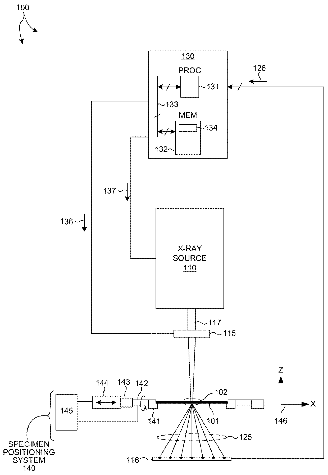
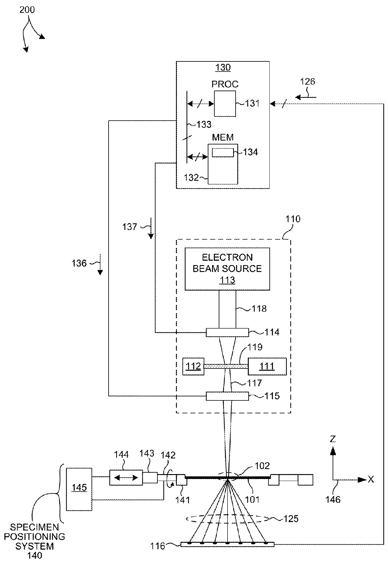
[0048]Methods and systems for characterizing dimensions and material properties of semiconductor devices by full beam x-ray scatterometry are described herein. Such systems and techniques are employed to measure structural and material characteristics associated with different semiconductor fabrication processes. In some examples, full beam x-ray scatterometry is employed to measure critical dimensions, thicknesses, overlay, and material properties of high aspect ratio semiconductor structures including, but not limited to, spin transfer torque random access memory (STT-RAM), three dimensional NAND memory (3D-NAND) or vertical NAND memory (V-NAND), dynamic random access memory (DRAM), three dimensional FLASH memory (3D-FLASH), resistive random access memory (Re-RAM), and phase change random access memory (PC-RAM).

[004...


PUM

PropertyMeasurementUnit
roughnessaaaaaaaaaa
aspect ratioaaaaaaaaaa
sizeaaaaaaaaaa

Abstract

Methods and systems for characterizing dimensions and material properties of semiconductor devices by full beam x-ray scatterometry are described herein. A full beam x-ray scatterometry measurement involves illuminating a sample with an X-ray beam and detecting the intensities of the resulting zero diffraction order and higher diffraction orders simultaneously for one or more angles of incidence relative to the sample. The simultaneous measurement of the direct beam and the scattered orders enables high throughput measurements with improved accuracy. The full beam x-ray scatterometry system includes one or more photon counting detectors with high dynamic range and thick, highly absorptive crystal substrates that absorb the direct beam with minimal parasitic backscattering. In other aspects, model based measurements are performed based on the zero diffraction order beam, and measurement performance of the full beam x-ray scatterometry system is estimated and controlled based on properties of the measured zero order beam.

Description

CROSS REFERENCE TO RELATED APPLICATION[0001]The present application for patent claims priority under 35 U.S.C. §119 from U.S. provisional patent application serial number 62 / 409,758, filed Oct. 18, 2016, the subject matter of which is incorporated herein by reference in its entirety.TECHNICAL FIELD[0002]The described embodiments relate to metrology systems and methods, and more particularly to methods and systems for improved measurement accuracy.BACKGROUND INFORMATION[0003]Semiconductor devices such as logic and memory devices are typically fabricated by a sequence of processing steps applied to a specimen. The various features and multiple structural levels of the semiconductor devices are formed by these processing steps. For example, lithography among others is one semiconductor fabrication process that involves generating a pattern on a semiconductor wafer. Additional examples of semiconductor fabrication processes include, but are not limited to, chemical-mechanical polishing,...

Claims


Application Information

Patent Timeline
Patent Type & Authority Applications(United States)
IPC IPC(8): G01N23/205G01B15/00G01N23/203
CPCG01N23/205G01N2223/6116G01N23/203G01B15/00H01J37/252H01J37/04G01B15/04G01N23/20066G01N23/2055G06T7/60G01N2223/05G01N2223/056G01N2223/302G01B2210/56G01N2223/0566
Inventor GELLINEAU, ANTONIO ARIONDZIURA, THADDEUS GERARDHENCH, JOHN J.VELDMAN, ANDREIZALUBOVSKY, SERGEY
Owner KLA CORP
Why Eureka
Try Eureka