
Nanowires or nanopyramids grown on graphitic substrate

a graphitic substrate and nanowire technology, applied in the direction of sustainable manufacturing/processing, climate sustainability, semiconductor devices, etc., can solve the problems of difficult deposition of conventional silica or silicon nitride masks on graphitic substrates, and the deposition method is not readily applicable to graphitic substrates

Active Publication Date: 2018-07-19
NORWEGIAN UNIVERSITY OF SCIENCE AND TECHNOLOGY (NTNU) +1
View PDF4 Cites 11 Cited by
  • Summary
  • Abstract
  • Description
  • Claims
  • Application Information

AI Technical Summary

Benefits of technology

The patent is about a way to transfer a layer of graphite with a seed layer and optionally a masking layer onto other surfaces. This can help in growing vertical nanowires or nanopyramids. The surface of the graphite substrate can also be modified to enhance the growth of nanowires or nanopyramids. In simpler terms, the patent describes a way to easily transfer and modify graphite layers for nanowire or nanopyramid growth.

Problems solved by technology

One problem, however, is that nanowires or nanopyramids can grow randomly on a substrate, in any position or in any direction.
The present inventors have realised, however, that the deposition of a conventional silica or silicon nitride mask on a graphitic substrate is problematic.
However, these deposition methods are not readily applicable to graphitic substrates.
Deposition of oxides or nitrides materials by CVD always involves the highly reactive oxygen or nitrogen radicals, which can easily damage the carbon bonds in graphene, leading to a serious loss of useful properties such as high electrical conduction.
The damage becomes more severe if the radicals are further activated in a plasma form in PE-CVD deposition.
This problem is quite similar in sputtering where highly accelerated oxides / nitrides elements in plasma bombards the graphitic surface.
This makes it difficult to deposit oxides and nitrides with e.g. H2O-based ALD technique, requiring complicated chemical functionalization of the graphene surface, which again degrades its properties.
The application of a thin seed layer on graphene for high quality oxide deposition is not new.
No one before, however, has considered the importance of the seed layer in the context of controlled growth of nanowires or nanopyramids on graphitic substrates.
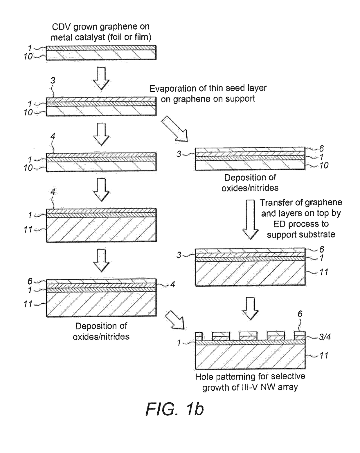
The inventors have noted that as-grown graphene with the metal catalyst underneath may not be readily used for NW growth.
For example, the use of CVD graphene grown on Cu cannot be used for NW growth as the Cu can cause severe contamination in the grown NWs, caused inter alia in the growth chamber from the evaporation and out-diffusion of Cu at high temperature.
CVD grown graphene on metal catalysts usually has local defects and micro- (or nano) cracks where the bottom metal surface is exposed.
The exposed metal surface can be highly reactive with semiconductor materials during the NW growth, which can overwhelm and destroy the proper NW growth on graphene surface.
The direct deposition of polymer-based materials on CVD grown graphene always leaves carbon residues on the surface, which results in carbon contamination during NW growth, degrading the doping control and optical properties of NWs as well as contaminating the growth system.
Any carbon residues on the seed or mask layers can be thoroughly cleaned by oxygen plasma treatment and wet chemical etching, which would easily destroy the bare graphene without seed or mask layers.

Method used


Image

  • Nanowires or nanopyramids grown on graphitic substrate
  • Nanowires or nanopyramids grown on graphitic substrate
  • Nanowires or nanopyramids grown on graphitic substrate

Examples


first embodiment

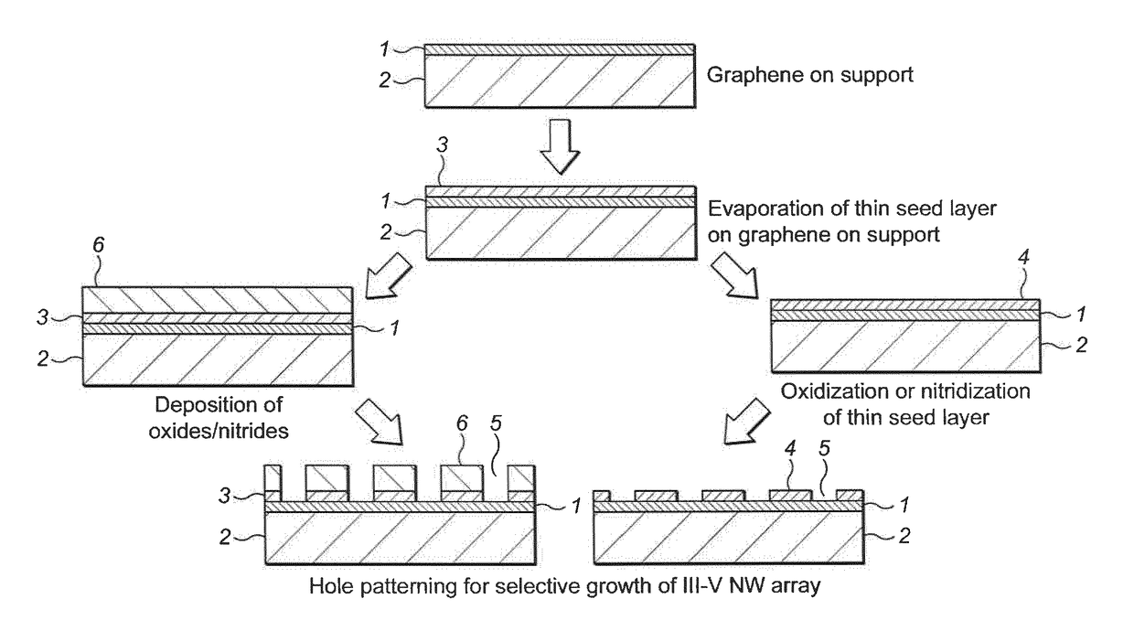
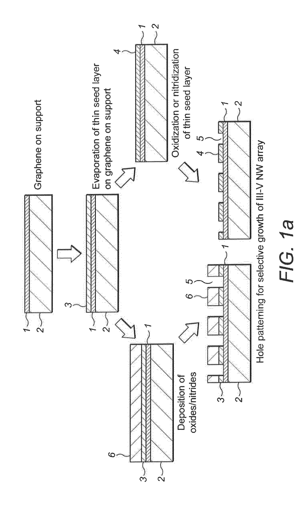
[0085]In the first embodiment, the seed layer is exposed to oxygen or nitrogen to cause oxidation or or nitridization of the seed layer to the corresponding oxide or nitride. The oxygen / nitrogen can be supplied as pure gas but more conveniently, it is simply supplied in air. The temperature and pressure of the oxidation process can be controlled to ensure that the seed layer oxidises / nitridizes but not the graphitic layer. Oxygen / nitrogen plasma treatment can be also applied. Preferred oxides are silicon dioxide, titanium dioxide or aluminium oxide.

second embodiment

[0086]In the second embodiment an oxide or nitride masking layer, preferably a metal oxide or metal nitride layer or semimetal oxide or semimetal nitride) is deposited on top of the seed layer. This can be achieved through atomic layer deposition or the techniques discussed above in connection with the deposition of the seed layer. The oxide used is preferably based on a metal or semimetal (such as Si). The nature of the cation used in the masking layer may be selected from the same options as the seed layer i.e. Al, Si or a transition metal, especially a first 3d row transition metal (Sc—Zn). The masking layer can therefore be formed from an oxide or a nitride of the seed layer element It is preferred if the metal atom of the seed layer (adjacent the masking layer) is the same as the cation of the masking layer. The masking layer should, however, be formed of a different material to the seed layer.

[0087]Preferred masking layers are based on oxides, such as SiO2, Si3N4, TiO2 or Al2O...

third embodiment

[0158]In a third embodiment, the problem of doping in an Al containing nanowire or nanopyramid is addressed using a tunnel junction. A tunnel junction is a barrier, such as a thin layer, between two electrically conducting materials. In the context of the present invention, the barrier functions as an ohmic electrical contact in the middle of a semiconductor device.

[0159]In one method, a thin electron blocking layer is inserted immediately after the active region, which is followed by a p-type doped AlGaN cladding layer with Al content higher than the Al content used in the active layers. The p-type doped cladding layer is followed by a highly p-type doped cladding layer and a very thin tunnel junction layer followed by an n-type doped AlGaN layer. The tunnel junction layer is chosen such that the electrons tunnel from the valence band in p-AlGaN to the conduction band in the n-AlGaN, creating holes that are injected into the p-AlGaN layer.

[0160]More generally, it is preferred if th...


PUM

PropertyMeasurementUnit
thicknessaaaaaaaaaa
thicknessaaaaaaaaaa
lengthaaaaaaaaaa

Abstract

A composition of matter comprising: a graphitic substrate optionally carried on a support; a seed layer having a thickness of no more than 50 nm deposited directly on top of said substrate, opposite any support; and an oxide or nitride masking layer directly on top of said seed layer; wherein a plurality of holes are present through said seed layer and through said masking layer to said graphitic substrate; and wherein a plurality of nanowires or nanopyramids are grown from said substrate in said holes, said nanowires or nanopyramids comprising at least one semiconducting group III-V compound.

Description

[0001]This invention concerns the fabrication of a hole patterned mask layer on a thin graphitic layer as a transparent, conductive and flexible substrate for nanowire or nanopyramid arrays preferably grown by a metal organic vapour phase epitaxy (MOVPE) method or molecular beam epitaxy (MBE) method. The graphitic substrate is provided with a seed layer which can be patterned to allow nanowire or nanopyramid growth in a patterned form such as a nanowire or nanopyramid array. Alternatively, the seed layer is itself provided with a masking layer which can be patterned (along with the seed layer) to allow nanowire or nanopyramid growth.[0002]The graphitic layer with seed and optionally masking layer on top can be transferred from a substrate onto other support surfaces, which may enhance vertical nanowire or nanopyramid growth.[0003]Over recent years, the interest in semiconductor nanowires has intensified as nanotechnology becomes an important engineering discipline. Nanowires, which ...

Claims


Application Information

Patent Timeline
Patent Type & Authority Applications(United States)
IPC IPC(8): H01L33/08H01L33/18H01L33/24H01L33/44H01L33/06H01L31/0352
CPCH01L33/08H01L33/18H01L33/24H01L33/44H01L33/06H01L31/035227H01L31/184H01L31/1852Y02E10/549Y02P70/50H10K71/191H10K71/166H01L33/0075H10K30/00
Inventor KIM, DONG CHULHOIAAS, IDA MARIE E.HEIMDAL, CARL PHILIP J.FIMLAND, BJORN OVE M.WEMAN, HELGE
Owner NORWEGIAN UNIVERSITY OF SCIENCE AND TECHNOLOGY (NTNU)
Learn More