Silicon carbide substrate production method and silicon carbide substrate

a silicon carbide substrate and production method technology, applied in the direction of superimposed coating process, crystal growth process, after-treatment details, etc., can solve the problems of high production cost of single crystal silicon carbide substrate, deformation of substrate, and limited application

Active Publication Date: 2019-12-19
SHIN ETSU CHEM IND CO LTD +1
View PDF0 Cites 4 Cited by
  • Summary
  • Abstract
  • Description
  • Claims
  • Application Information

AI Technical Summary

Benefits of technology

[0047]According to the present invention, a polycrystalline silicon carbide film is formed on a covering layer of a support substrate having a smooth surface without eroding the covering layer, and therefore, a polycrystalline silicon carbide film having a surface reflecting the smooth surface of the support substrate can be obtained as a silicon carbide substrate.

Problems solved by technology

A single crystal Si substrate has been used so far as a main substrate for a dummy wafer of a semiconductor process, a mold material for nanoimprinting or the like, a mirror, a membrane material for X-ray lithography, or micro electro mechanical systems (MEMS), however, the application has been limited because the mechanical strength, the chemical durability, and the heat resistance are insufficient.
In this regard, in a case where a single crystal silicon carbide substrate is used for the application, the production cost of the single crystal silicon carbide substrate is high, and if a thermal process or the like is performed, a problem that dislocation in the crystal glides to cause deformation of the substrate is generated.
However, when chemical-mechanical polishing (CMP) is applied onto a surface of a substrate in order to obtain a smooth surface, a problem that the smoothness on the surface is impaired is caused.
However, there are some concerns, for example, that the processing processes become complicated, that the processing quality changes due to the electric conductivity, and that pits are generated at locations of crystal defects.
However, in this method, since thermal stress is applied to the silicon carbide, movement and extension of defects in the crystal are promoted, and a problem that the desired quality cannot be obtained is concerned.
However, there are some problems, for example, that the production processes become complicated, that the quality of crystal is deteriorated due to the high temperature treatment, that the grain size of the surface is limited, and that boron is incorporated as an impurity.
However, it is not easy to make the orientation of crystal grains of the polycrystalline thin film coated on the surface of the base body isotropic, and further a problem that the smoothness of the surface of the polycrystalline silicon carbide film is influenced by the surface roughness of the polycrystalline thin film coated on the surface of the base body is generated.

Method used


Image

  • Silicon carbide substrate production method and silicon carbide substrate
  • Silicon carbide substrate production method and silicon carbide substrate
  • Silicon carbide substrate production method and silicon carbide substrate

Examples


example 1

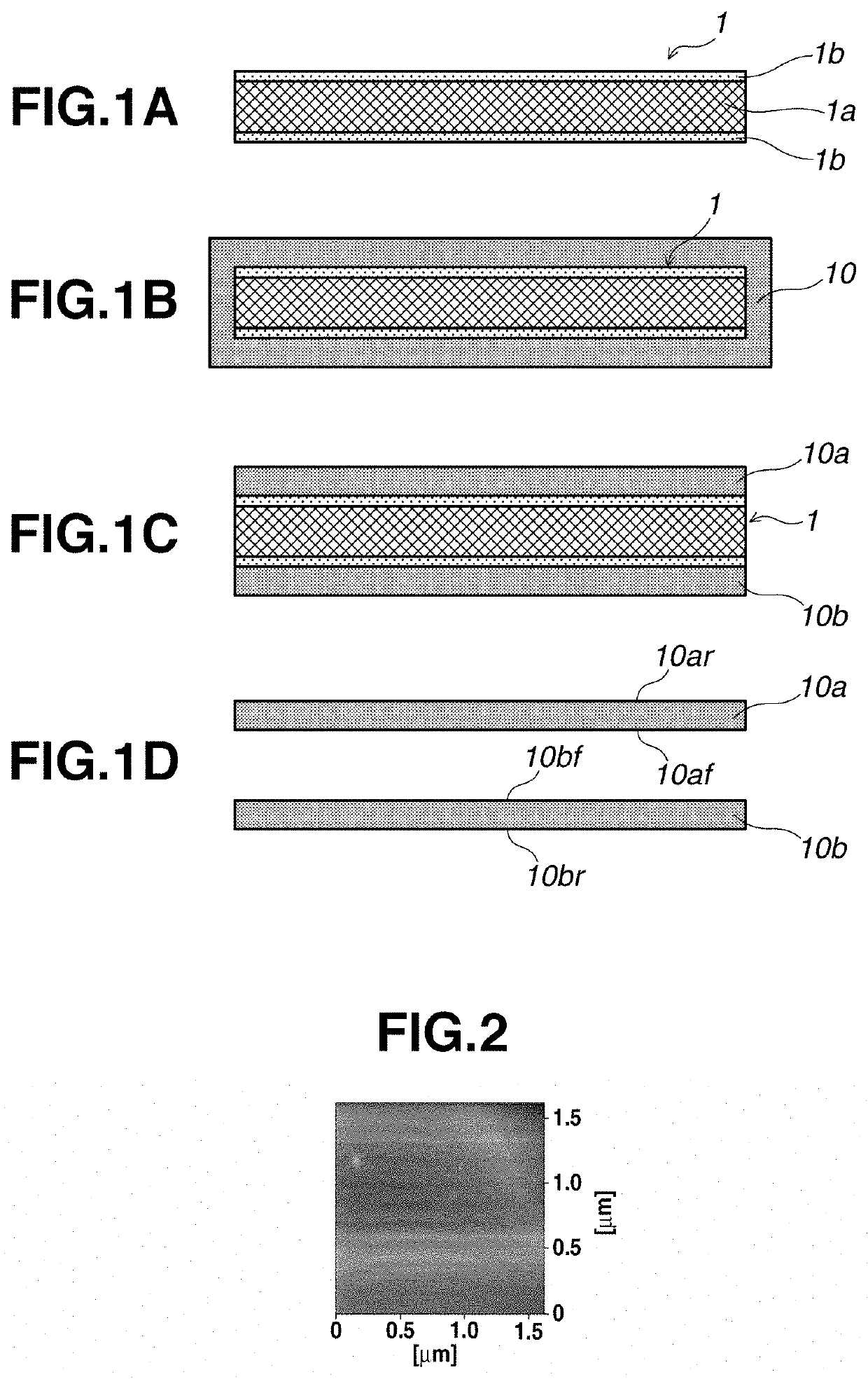
[0119]A silicon carbide substrate was prepared by the procedure shown FIG. 1.

[0120]First, as a base substrate 1a, a single crystal silicon substrate having a diameter of 3 inches, a thickness of 400 μm, and a surface of (100) plane was used. Both surfaces of the silicon substrate were polished, and the arithmetic mean roughness Ra of the substrate surface was 0.1 nm.

[0121]Next, the silicon substrate was subjected to a wet oxidation treatment at 1,100° C., and thermal oxide films each having a thickness of 0.5 μm were formed as covering layers 1b and 1b on the front and back surfaces of the substrate to prepare a support substrate 1. In this case, the surfaces of the covering layers 1b and 1b (thermal oxide films) reflect the smooth surfaces of the base substrate 1a (silicon substrate), and the arithmetic mean roughness Ra of the surface of the support substrate 1 was 0.3 nm or less.

[0122]Next, the silicon carbide film was formed on the support substrate 1 by using a thermal CVD meth...

example 2

[0131]A silicon carbide substrate was prepared by the procedure shown FIG. 1.

[0132]First, as a base substrate 1a, a high-purity carbon substrate having a diameter of 3 inches and a thickness of 400 μm was used. The arithmetic mean roughness Ra of the surface of the carbon substrate was 2.3 nm.

[0133]Next, boro-phospho silicate glass (BPSG) films each having a thickness of 1 μm were deposited on the front and back surfaces of the carbon substrate as covering layers 1b and 1b by a CVD method. Subsequently, by heating to 900° C. in an argon gas atmosphere, the covering layers 1b and 1b were reflowed to obtain a support substrate 1 with smoothed surfaces. The arithmetic mean roughness Ra of the surface of this support substrate 1 was 0.2 nm.

[0134]Next, a silicon carbide film having a thickness of 300 μm was formed on the support substrate 1 under the same conditions as in Example 1 by using a thermal CVD method.

[0135]Subsequently, the silicon carbide film deposited to the end parts of th...


PUM

PropertyMeasurementUnit
roughnessaaaaaaaaaa
crystal grain sizeaaaaaaaaaa

Abstract

A silicon carbide substrate production method includes: the step of providing covering layers 1b, 1b, each containing silicon oxide, silicon nitride, silicon carbonitride, or silicide, respectively on both surfaces of a base material substrate 1a carbon, silicon or silicon carbide, and turning the surface of each of the covering layers 1b, 1b into a smooth surface to prepare a support substrate 1; a step of forming a polycrystalline silicon carbide film 10 on both surfaces of the support substrate 1 by a gas phase growth method or a liquid phase growth method; and a step of separating the polycrystalline silicon carbide films from the support substrate while preserving, on the surface thereof, the smoothness of the covering layer surfaces 1b, 1b by chemically removing at least the covering layers 1b, 1b, from the support substrate 1. The silicon carbide substrate has a smooth surface and reduced internal stress.

Description

TECHNICAL FIELD[0001]The present invention relates to a method for producing a silicon carbide substrate having a flat and smooth surface, and to a silicon carbide substrate.BACKGROUND ART[0002]A single crystal Si substrate has been used so far as a main substrate for a dummy wafer of a semiconductor process, a mold material for nanoimprinting or the like, a mirror, a membrane material for X-ray lithography, or micro electro mechanical systems (MEMS), however, the application has been limited because the mechanical strength, the chemical durability, and the heat resistance are insufficient. Recently, as a substrate used for the application, a silicon carbide substrate that is excellent in the heat resistance, and the mechanical properties, and is resistant to radiation has been attracting attention.[0003]The substrate to be used for the application is required to have a smoothness such that the total thickness variation (TTV) is 50 μm or less and the arithmetic mean roughness Ra is ...

Claims


Application Information

Patent Timeline
Patent Type & Authority Applications(United States)
IPC IPC(8): C30B29/36H01L21/02H01L21/683H01L29/16C30B25/18C30B33/10
CPCC30B33/10H01L2221/68381C30B25/18H01L21/6835H01L21/0262C30B29/36H01L29/1608H01L21/02595H01L2221/68345H01L21/02529H01L21/02378H01L21/02488H01L21/02005H01L21/02167H01L21/02271H01L21/02269H01L21/205C30B25/186C30B25/20C30B25/22C23C16/01C23C16/0272C23C16/325C23C28/04C23C28/42C23C28/44H01L21/02447H01L21/02658
Inventor NAGASAWA, HIROYUKIKUBOTA, YOSHIHIROAKIYAMA, SHOJI
Owner SHIN ETSU CHEM IND CO LTD
Why Eureka
Try Eureka