

Semiconductor device having ultra-sharp P-N junction and method of manufacturing the same
a semiconductor and ultra-sharp technology, applied in the direction of semiconductor devices, diodes, electrical devices, etc., can solve the problems of not being able to provide a high-conductivity diode built on top of a metal conductor at the same time, and detracting from the signal being sensed
- Summary
- Abstract
- Description
- Claims
- Application Information
AI Technical Summary
Benefits of technology
Problems solved by technology
Method used
Image

Examples
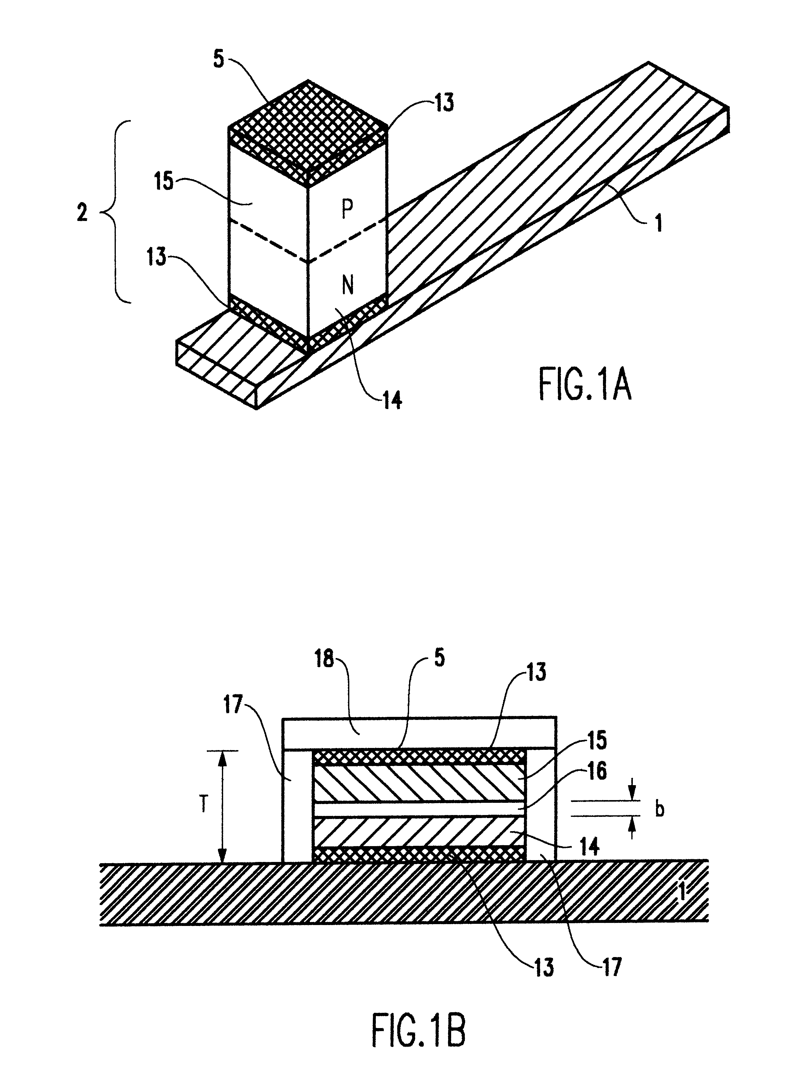
first embodiment
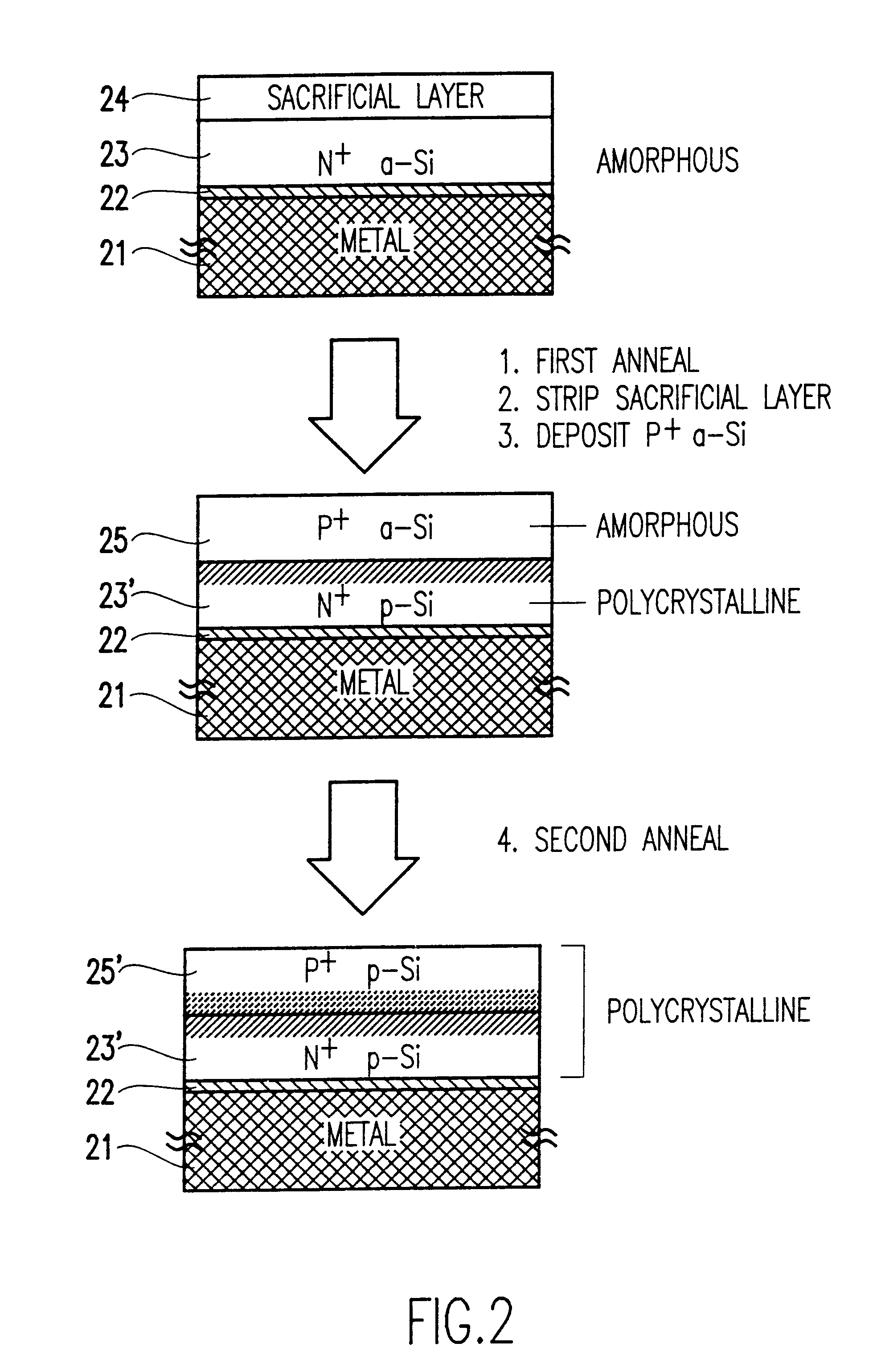
Referring to FIG. 2, the method of the present invention for making the confined P-N junction is now described. In FIG. 2, both the N and P dopants are placed in situ during a-Si deposition, but there are two separate deposition steps. The stepwise formation method is described below.
First, contact layer 22 is formed on a metal layer 21 (which is equivalent to metal line 1 in FIGS. 1A-1B). Then, a layer 23 of N.sub.+ a--Si (e.g., the first layer) is deposited on the contact layer 22 (e.g., layer 22 is equivalent to lower layer 13 in FIG. 1B). The contact layer 22 preferably has a thickness in the range of 0.005 to 0.05 and more preferably 0.01 to 0.03 microns.
Optionally, the contact layer 22 may include first and second sublayers. The first sublayer contacting the metal line 21 is a diffusion barrier (e.g., TiN or SiTaN or Ta), and the second sublayer contacting the semiconductor layer 23 is a very highly doped semiconductor. Layer 23 preferably has a thickness in the range of 0.05 ...
second embodiment
The second embodiment differs from the first embodiment by using no sacrificial layer, and requiring only one ion implantation step.
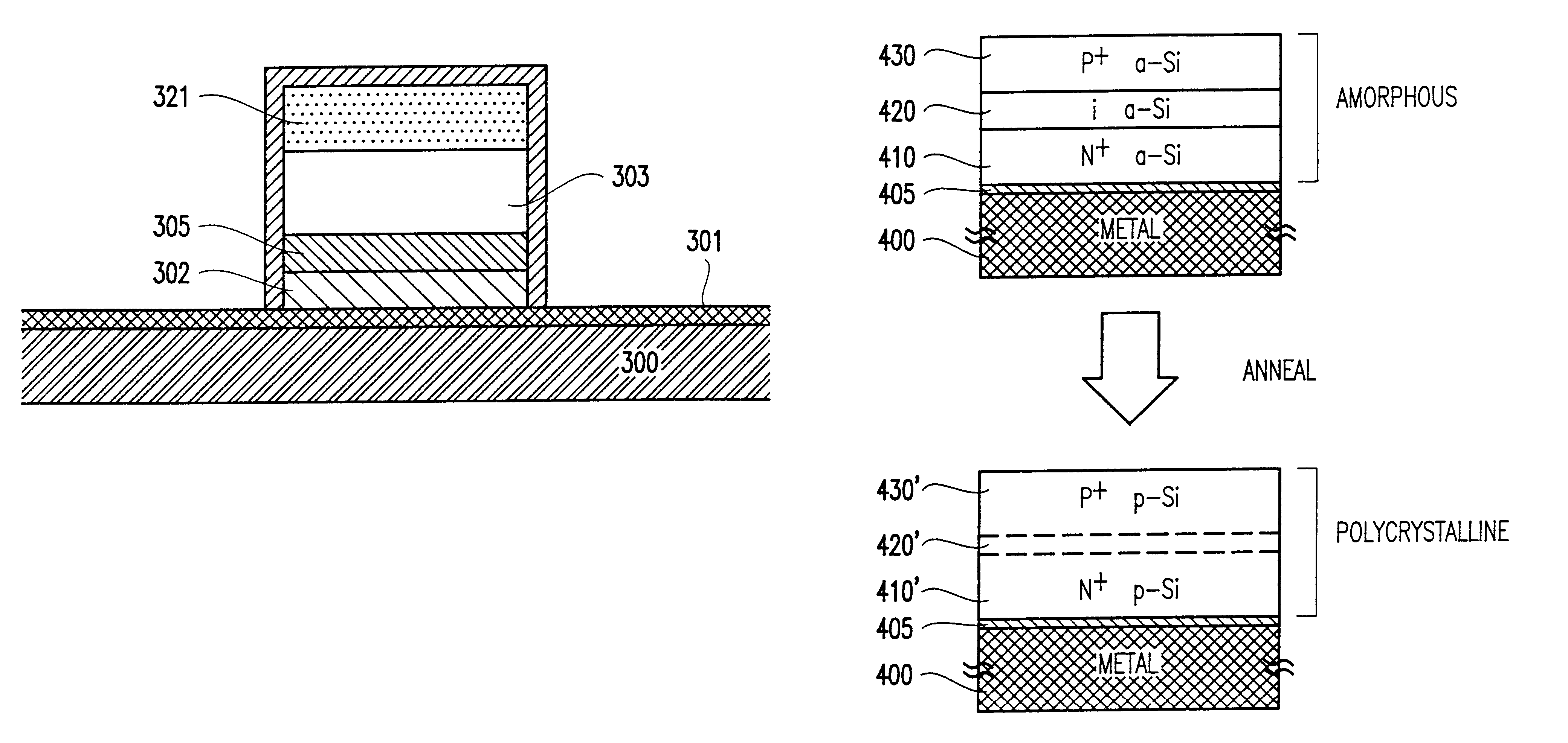
In FIG. 3A, the metal address line 300 has been deposited and patterned. Metal line 300 preferably comprises aluminum, copper, tungsten and alloys such as AlCu, TiW, or other metals.
Optionally, a diffusion barrier layer 301 is placed on top of the metal line 300. The diffusion barrier layer 301 may be TiN, SiTaN, or Ta.
Then, two layers of amorphous Si are deposited in a single procedure using either plasma-enhanced chemical vapor deposition (PECVD), reactive magnetron sputtering, or low pressure chemical vapor deposition (LPCVD).
First, a layer 302 of a--Si highly-doped with N dopant (e.g., phosphorous, antimony or arsenic is deposited.
Then without exposure to atmosphere a layer 303 of undoped, intrinsic a-Si is deposited in the same deposition chamber. Preferably, the thickness of layer 302 is within a range of approximately 0.01-0.05 microns, and the t...
third embodiment
The third embodiment differs from the first and second embodiments by performing deposition of all layers in a single step, and by eliminating sacrificial layer and ion implantation steps.
Referring to FIG. 4, both the N and P dopants are placed in situ during a-Si deposition, in a single Si deposition step.
Optionally, a diffusion barrier layer 405 composed of TiN or SiTaN or Ta is placed on a metal line 400.
First, three layers 410, 420, and 430 are deposited in a single vacuum pumpdown (e.g., N.sup.+ a--Si, intrinsic a--Si, P.sup.+ a--Si) in a single deposition tool, on the metal line 400. Preferably, layer 410 has a thickness within a range of approximately 0.01 to 0.2 microns, and more preferably in a range of 0.05 to 0.1 microns. Layer 420 preferably has a thickness within a range of approximately 0.01 to 0.3 microns, and more preferably in a range of 0.01 to 0.1 microns. Layer 430 preferably has a thickness within a range of approximately 0.01 to 0.2 microns, and more preferably...
PUM
 Abstract
Description
Claims
Application Information