Low-cost 3D flip-chip packaging technology for integrated power electronics modules

a technology of power electronics module and flip-chip, which is applied in the direction of solid-state devices, basic electric elements, electrical apparatus construction details, etc., can solve the problems of high resistance and parasitics, poor thermal management, and high cos

Inactive Publication Date: 2002-08-27
VIRGINIA TECH INTPROP INC
View PDF13 Cites 91 Cited by
  • Summary
  • Abstract
  • Description
  • Claims
  • Application Information

AI Technical Summary

Benefits of technology

It is another object of the invention to provide a generalized packaging structure for power modules which will support improved performance of the devices while accommodating inclusion of low power control and protection devices, including condition sensors.
It is a further object of the invention to provide a power semiconductor device packaging which includes chip scale packaging to reduce cost and improve performance.
It is yet another object of the invention to provide an improved solder bump structure and process for improving durability to withstand extreme thermal cycling over long periods of service.

Problems solved by technology

However, development of packaging for semiconductor power control devices, referred to as power modules, has not kept pace with the development of packaging for digital circuits and, moreover, requires consideration of a much wider variety of operating conditions and device characteristics than for digital processing and memory circuits having relatively low power requirements and which are not required to deliver significant power levels to an external device.
At the present time, most packaging for power modules is in one of the well-known forms of single in-line packages (SIP), dual in-line packages (DIP), small outline packages (SO / SOP) and quad flat packs (QFP) all of which have been known for a number of years, have high resistance and parasitics, poor thermal management and high cost.
Wire bonds in power modules are not only subject to high resistance and noise but also parasitic oscillations, fatigue and eventual failure.
That is, where the power modules are switching at high di / dt and dv / dt, the connections generate strong electromagnetic fields, resulting in proximity effects and uneven current distribution among bonding wires as well as excess parasitic inductance which can increase the voltages the devices must withstand as large currents are reduced at a rapid rate.
From the point of view of reliability, wire bonding has proven to be one of the weakest areas of power module packaging since high current requires thick 0.25-0.50 mm wires to be employed for wire bonds.
One of the main failure mechanisms in high power devices such as insulated gate bipolar transistors (IGBT) modules subject to thermal cycling is wire bond lift-off due to the large coefficient of thermal expansion (CTE) mismatch between metal (e.g. aluminum) wires and silicon chips.
Wire bonds may also be effectively damaged by the unavoidable deformation and working of the wire during the bonding process that may generate small dimensional differences that concentrate heat generation and mechanical stress.
Motion of the wires to accommodate CTE mismatch during thermal cycling and due to proximity effects cumulatively contribute to fatigue of both the wire and the bond.
Therefore, the mean time to failure of power modules is often foreshortened while increased service lifetimes are demanded (e.g. about thirty years) which cannot be achieved with current package technologies, especially including wire bonds.
In summary, current packaging technology effectively limits performance of current power chips and recent technical developments have not provided overall improvements in performance while available packaging technology does not allow exploitation of the full potential of recent advances in power chips or to support future power chips.

Method used


Image

  • Low-cost 3D flip-chip packaging technology for integrated power electronics modules
  • Low-cost 3D flip-chip packaging technology for integrated power electronics modules
  • Low-cost 3D flip-chip packaging technology for integrated power electronics modules

Examples


first embodiment

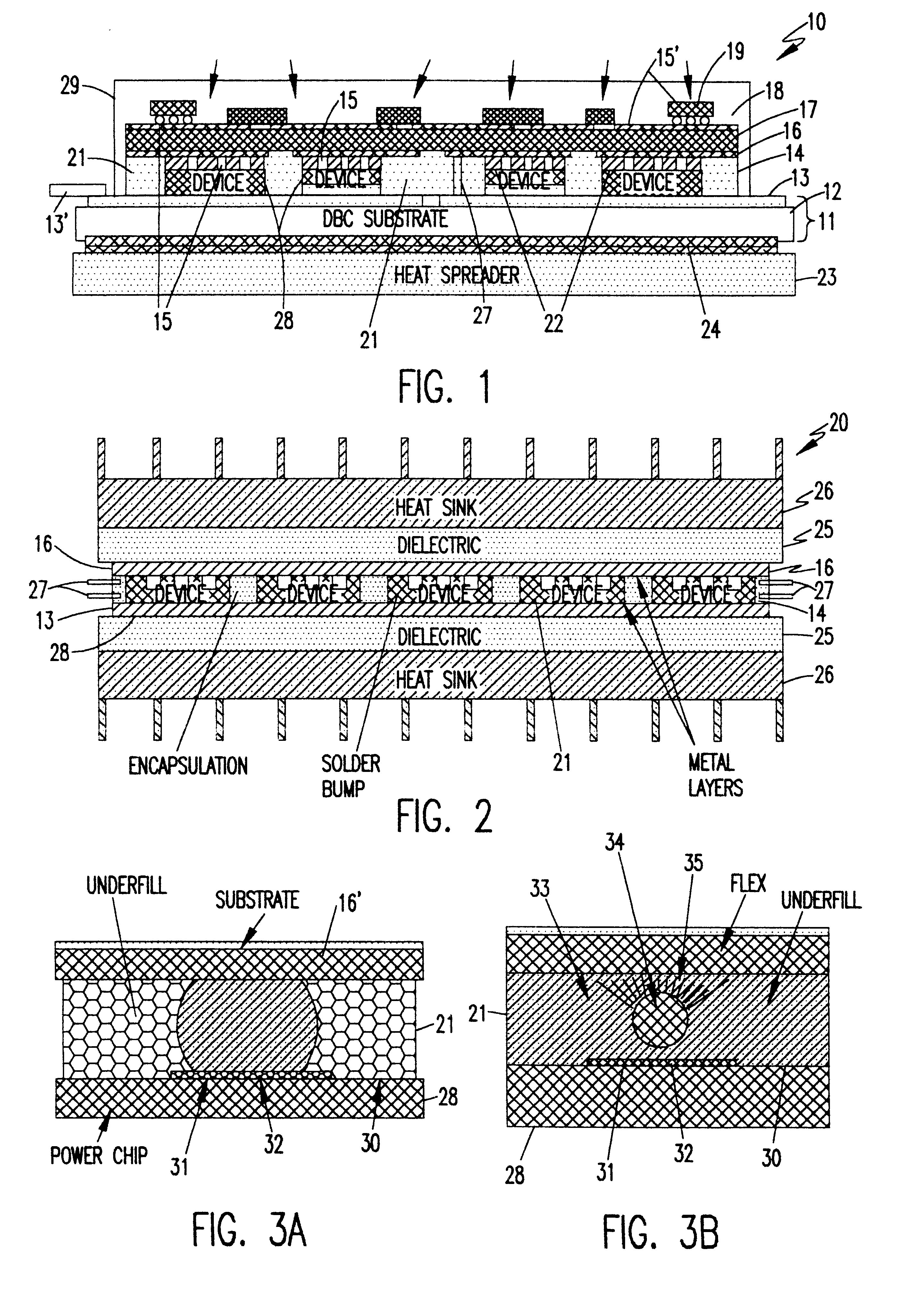
FIG. 1 includes a first plate 11 including a heat conducting substrate such as Burquist board (a laminate comprising a relatively thick layer of aluminum 12, a thin layer of insulating polyimide or other dielectric and a layer 13 of copper of arbitrary thickness), direct bond copper (DBC) on both sides of an aluminum nitride (AlN) substrate which has a CTE closely matched to silicon or other insulated metal substrate. The metal layers should be sufficiently thick (and symmetrical) to provide adequate thermal and electrical conduction (while thin enough to avoid alteration of dimensional change with temperature of the assembly with aluminum nitride) and the insulator layers should be adequately thin to avoid compromise of thermal conduction between the metal layers.

The copper layer 12 may thus be patterned as required to provide interconnections, shielding and the like. The second plate comprises a layer of metal (e.g. copper) 16, an insulator layer 17 and a second metal (e.g. copper...
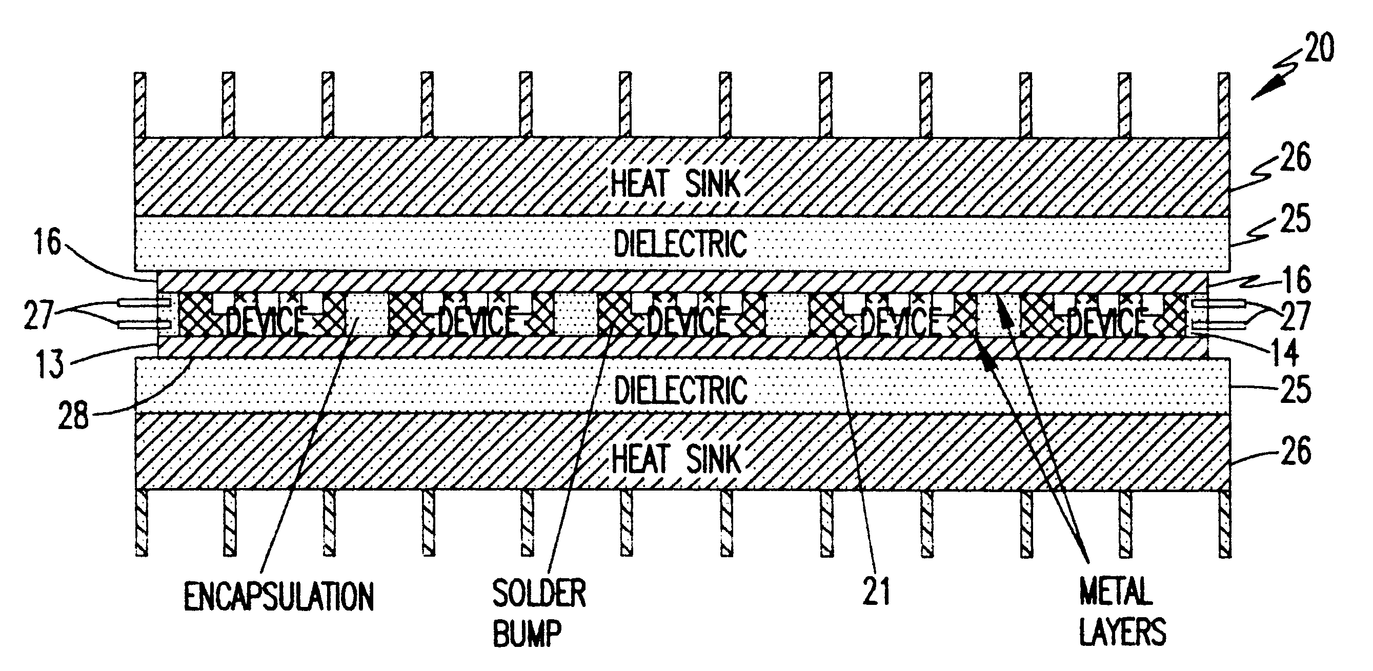
second embodiment

Moreover, but for the orientation of power devices 28, the structure is entirely symmetrical to further avoid the development of internal stresses. The orientation of the power devices is unimportant in view of the heat conduction and compliance of the encapsulant. As a perfecting feature of the invention, all of the power device could be made or CSP packaging applied to develop a substantially uniform height for improved heat conduction to surface 13. Power bus connections 27 can be made through the encapsulation at any point on the periphery of the device or even through the heat sinks 26 and dielectric 25, if desired.

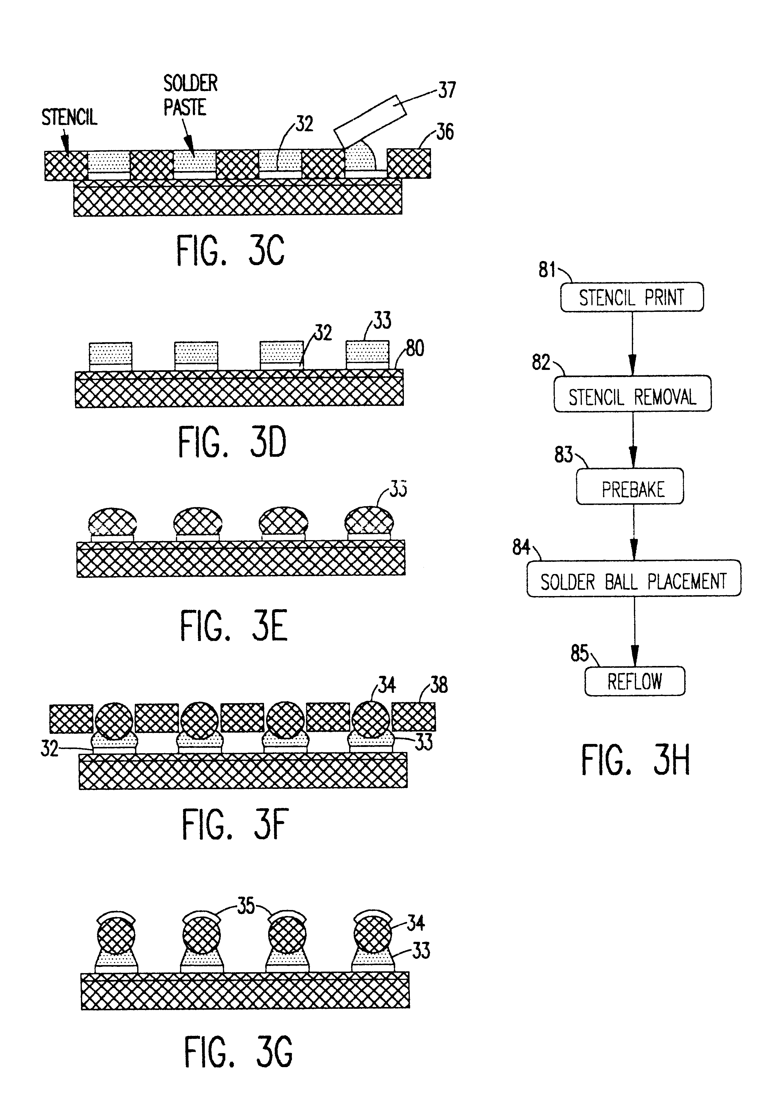
Referring now to FIGS. 3A, 3B acceptable and preferred forms of the solder balls will now be discussed. The solder ball form shown in FIG. 3A is conventional in topology but not necessarily in scale. The structure illustrated in FIGS. 3A and 3B include a passivation film on the surface of power device 28, as is customary. An aluminum pad 31 is formed in an aperture i...


PUM


Abstract

Resistance and parasitic inductance resulting from interconnection of semiconductor chips in power modules are reduced to negligible levels by a robust structure which completely avoids use of wire bonds through use of ball bonding and flip-chip manufacturing processes, possibly in combination with chip scale packaging and hourglass shaped stacked solder bumps of increased compliance and controlled height / shape. Turn-off voltage overshoot is reduced to about one-half or less than a comparable wire bond packaged power module. Hourglass shaped solder bumps provide increased compliance and reliability over much increased numbers of thermal cycles over wide temperature excursions.

Description

1. Field of the InventionThe present invention generally relates to packaging of semiconductor integrated circuits for medium-level power applications such as inverters for motor drives and convertors for processing equipment and, more specifically, to modular structures for power semiconductor devices and associated integrated circuits.2. Description of the Prior ArtVirtually all semiconductor electronic devices from discrete diodes and transistors to integrated circuits of very high integration density require packaging or encapsulation for mechanical protection and support as well as thermal control. In digital logic devices, packaging has been developed quite extensively and is highly sophisticated at the present state of the art; often providing for multi-chip modules containing many interconnected chips or dies. Thermal control has been critical to support high switching speeds of such circuits which may include millions of active devices on a single chip.However, development ...

Claims


Application Information

Patent Timeline
Patent Type & Authority Patents(United States)
IPC IPC(8): H01L21/02H01L21/56H01L23/485H01L23/48H01L23/52H01L23/538
CPCH01L21/563H01L23/5385H01L24/11H01L2924/1305H01L2924/00014H01L2924/10253H01L2224/45124H01L2924/014H01L2924/01033H01L2924/01006H01L2224/11003H01L2224/13099H01L2224/73203H01L2924/01013H01L2924/01022H01L2924/01029H01L2924/01047H01L2924/01078H01L2924/01082H01L2924/01322H01L2924/13055H01L2924/13091H01L2924/14H01L2924/19041H01L2924/19043H01L2924/30107H01L2924/3025H01L2924/00H01L2224/48H01L2924/181H01L2924/12036H01L2224/05573H01L2224/05568H01L2224/056H01L24/05
Inventor LIU, XINGSHENGLU, GUO-QUAN
Owner VIRGINIA TECH INTPROP INC
Why Eureka
Try Eureka