

Method of manufacturing a thin film transistor-integrated color filter
a technology of thin film transistors and color filters, applied in the field of color filter manufacturing, can solve the problems of high cost, high number of steps, poor resolution power or uniform film thickness, etc., and achieve the effect of improving the position accuracy, high possibility of mixing color in adjacent filter layers, and improving the quality of the filter
- Summary
- Abstract
- Description
- Claims
- Application Information
AI Technical Summary
Benefits of technology
Problems solved by technology
Method used
Image

Examples
example 1
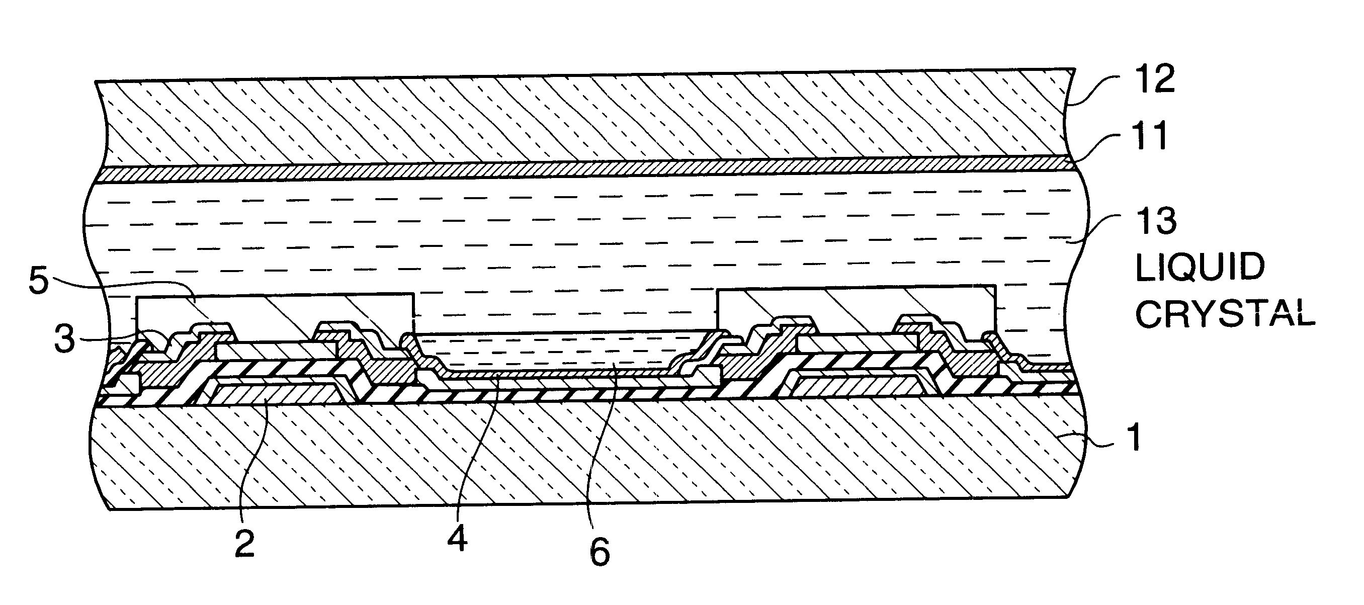
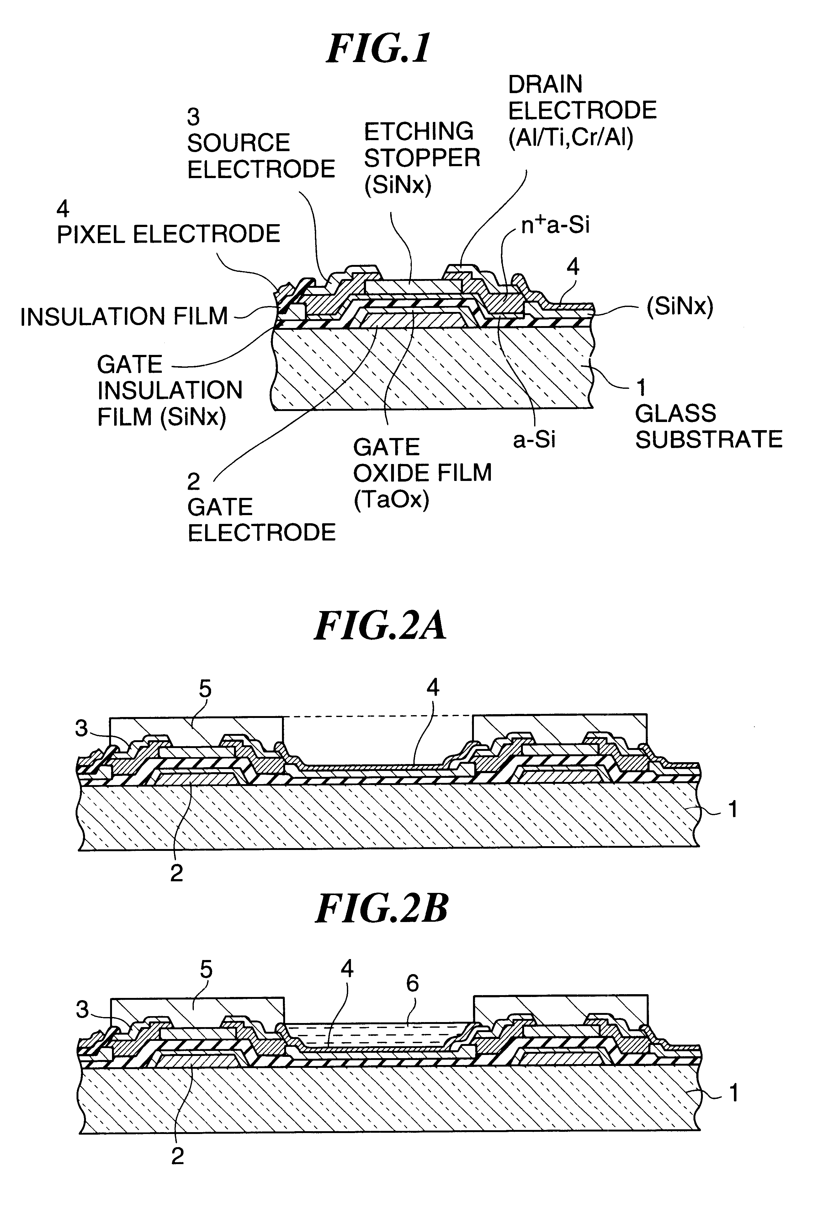
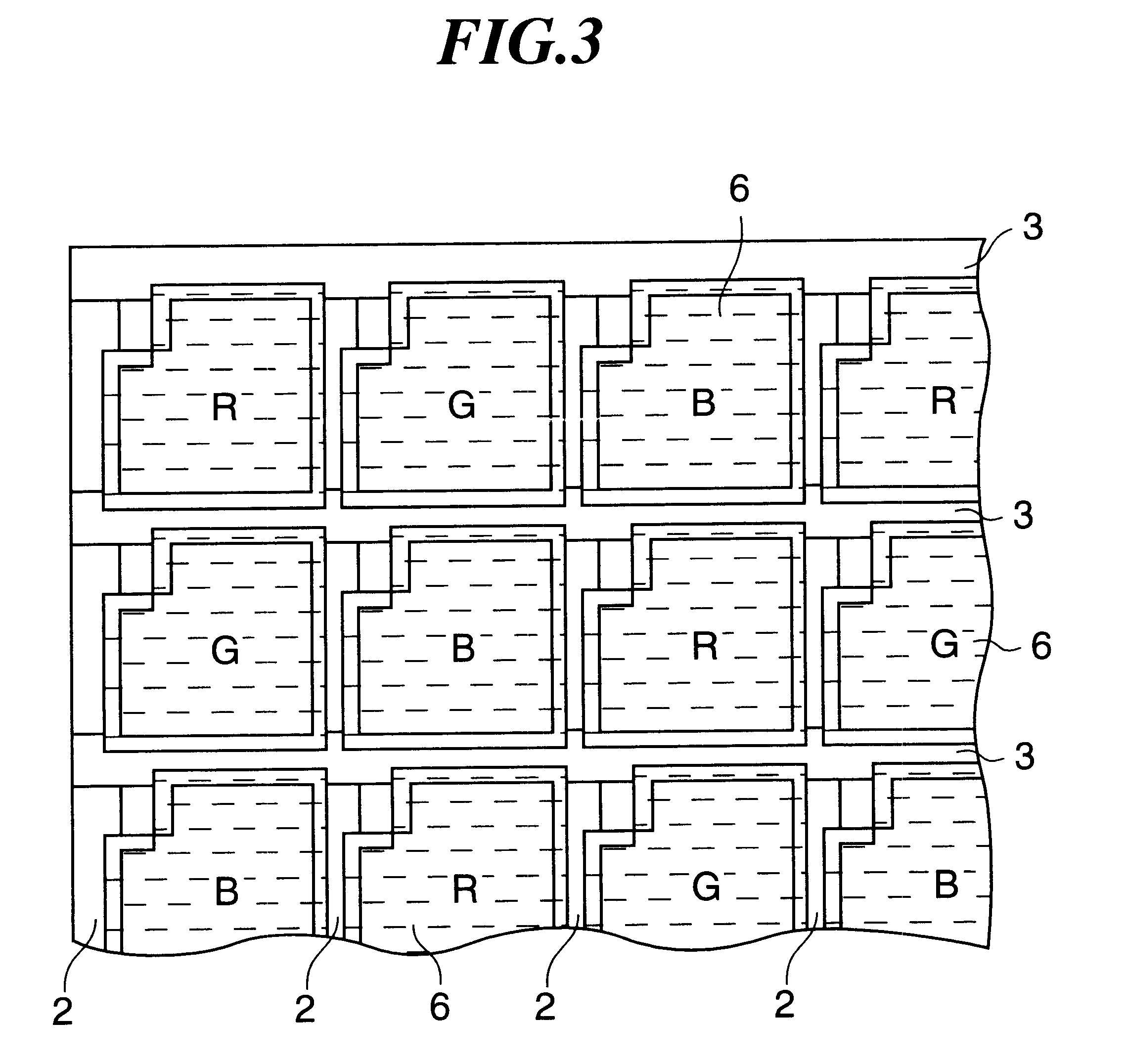
As shown in FIG. 1, a thin film transistor (TFT) and a pixel electrode of a transparent conductive film (ITO) were formed on an alkaline glass substrate of 0.7 m in thickness (1737 glass manufactured by Corning Inc.). In this case, the gate electrode and the drain electrode of the TFT were formed of a two-layered chromium film. After disposing an insulation layer with silicon nitride so that the electrode and power source line portions can be used both as a black matrix after forming the color filter layer, the ITO was extended upon forming the pixel electrode so as to overlap the power source line to thereby eliminate a transparent region other than the pixel electrode, which was utilized as a TFT substrate (manufacturing step of substrate for use in liquid crystal display).
Then, in a state of applying a voltage to the gate electrode of the TFT substrate such that red is entirely indicated upon liquid crystal display, a substrate was brought into contact with an electrodeposition s...
example 2
As shown in FIG. 1, a thin film transistor (TFT) and a pixel electrode of a transparent conductive film (ITO) are formed on an alkaline glass substrate of 0.7 mm in thickness (1737 glass manufactured by Corning Inc.) (manufacturing step of substrate for use in liquid crystal display).
Then, a positive type black resist was coated on the TFT substrate, light is irradiated from the back surface of the substrate and only the light irradiated region was etched to expose a pixel electrode (black matrix forming step).
Then, in a state of applying a voltage to of the TFT substrate such that red in entirely indicated upon liquid crystal display, the substrate was brought into contact with an electrodeposition solution (pH=7.9. conductivity=10 mS / cm) containing a styrene-acrylic acid copolymer (molecular weight: 13,000, hydrophilic group / (hydrophobic group+hydrophilic group) molar ratio: 65%, acid value: 150) and an azo series red super-micro particle pigment at a 1:2 solid content ratio, and ...
example 3
As shown in FIG. 1, a thin film transistor (TFT) and a pixel electrode of a transparent electrode conductive film (ITO) were formed on an alkaline glass substrate (1737 glass manufactured by Corning Inc.) of 0.7 mm in thickness. In this case, the gate electrode and the drain electrode of the TFT were formed of two layered chromium files to provide the electrode with low reflectivity and light shielding property (manufacturing step for substrate for use in liquid crystal display).
The positive type resist was coated on the TFT substrate, a light war irradiated on the back surface of the substrate and only the light irradiation region was etched to expose the pixel electrode. Then, in a state of applying a voltage to the gate electrode of the TFT substrate such that red is entirely indicated upon liquid crystal display, a substrate was brought into contact with an electrodeposition solution (pH=7.8. conductivity=10 mS / cm) containing a styrene-acrylic acid copolymer (molecular weight: 1...
PUM
| Property | Measurement | Unit |
|---|---|---|
| voltage | aaaaa | aaaaa |
| voltage | aaaaa | aaaaa |
| voltage | aaaaa | aaaaa |
Abstract
Description
Claims
Application Information