Method of electroplating a copper-zinc alloy thin film on a copper surface using a chemical solution

a technology of copper-zinc alloy and chemical solution, which is applied in the direction of electrolysis process, semiconductor devices, electrolysis components, etc., can solve the problems of not providing a cost-effective method of forming a copper-zinc alloy on a cu interconnect surface, and less desirable as a candidate for these higher density devices, etc., to achieve enhanced filling capability, reduce the resistance of the formed cu-zn alloy, and improve the effect of filling

Inactive Publication Date: 2003-03-04
ADVANCED MICRO DEVICES INC
View PDF6 Cites 4 Cited by
  • Summary
  • Abstract
  • Description
  • Claims
  • Application Information

AI Technical Summary

Benefits of technology

The present Cu--Zn electroplating solution facilitates better filling of a Cu--Zn alloy thin film on an interconnect, especially for feature sizes in a dimensional range of approximately 0.2 .mu.m to approximately 0.05 .mu.m, thereby lowering the resistance of the formed Cu--Zn alloy thin film (e.g., in a resistance range of approximately 2.2 .mu..OMEGA..multidot.cm to approximately 2.5 .mu..OMEGA.cm for approximately 1 at. % Zn content in a Cu--Zn alloy thin film, as deposited). Further, the filling capability is enhanced by three beneficial characteristics of the present invention: (1) the instant chemical solution does not etch copper or a copper alloy seed layer; (2) the introduction of Zn into the alloy thin film as well as onto the Cu interconnect improves both step coverage and nucleation; and (3) a variety of organic additives, ...

Problems solved by technology

Despite aluminum's (Al) adequate resistance, other Al properties render it less desirable as a candidate for these higher density devices, especially with respect to its deposition into plug regions having a high aspect ratio cross-sectional area.
However, some disadvantages of using Cu as an interconnect material include etching problems, corrosion, and diffusion into silicon..sup.1 These ...

Method used


Image

  • Method of electroplating a copper-zinc alloy thin film on a copper surface using a chemical solution
  • Method of electroplating a copper-zinc alloy thin film on a copper surface using a chemical solution
  • Method of electroplating a copper-zinc alloy thin film on a copper surface using a chemical solution

Examples


Embodiment Construction

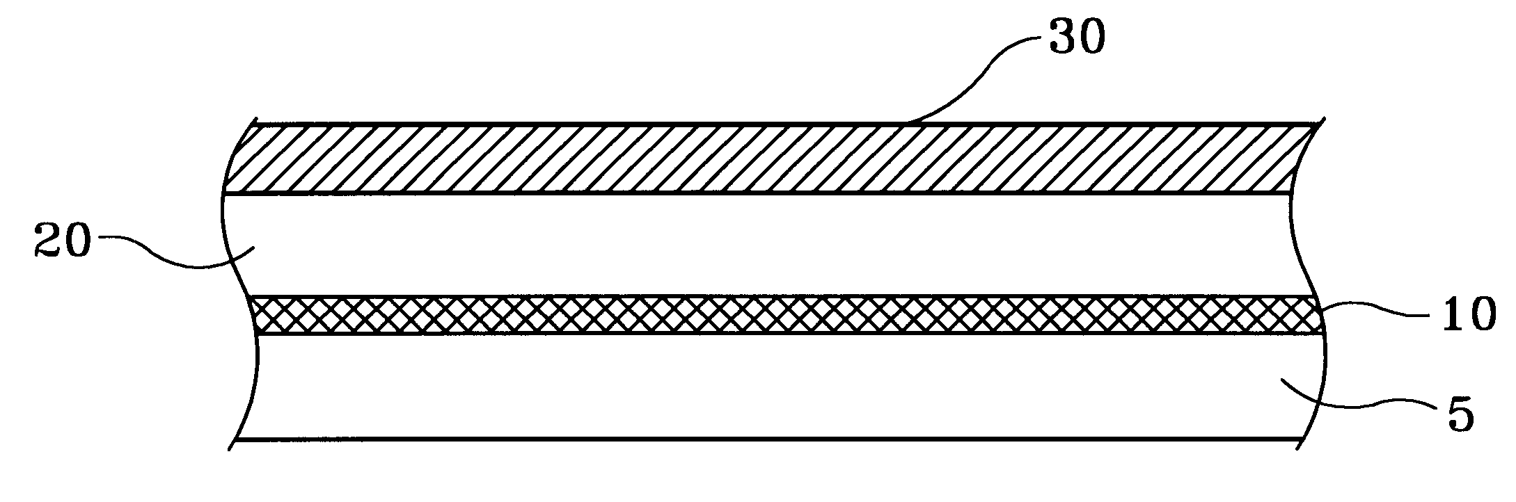
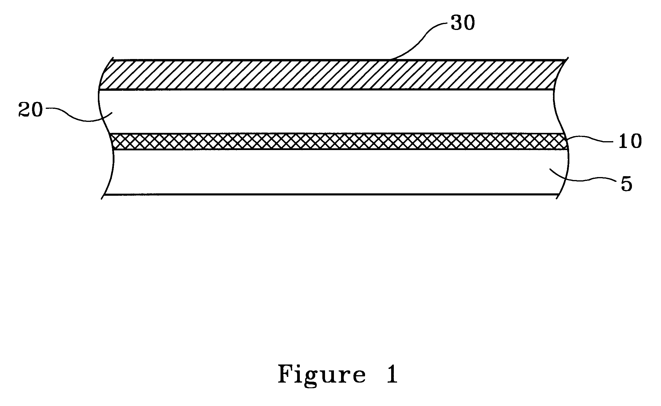
FIG. 1 illustrates, by example only, and in cross-section, a Cu surface 20 having been deposited with a Cu--Zn alloy thin film 30, in accordance with the present invention.

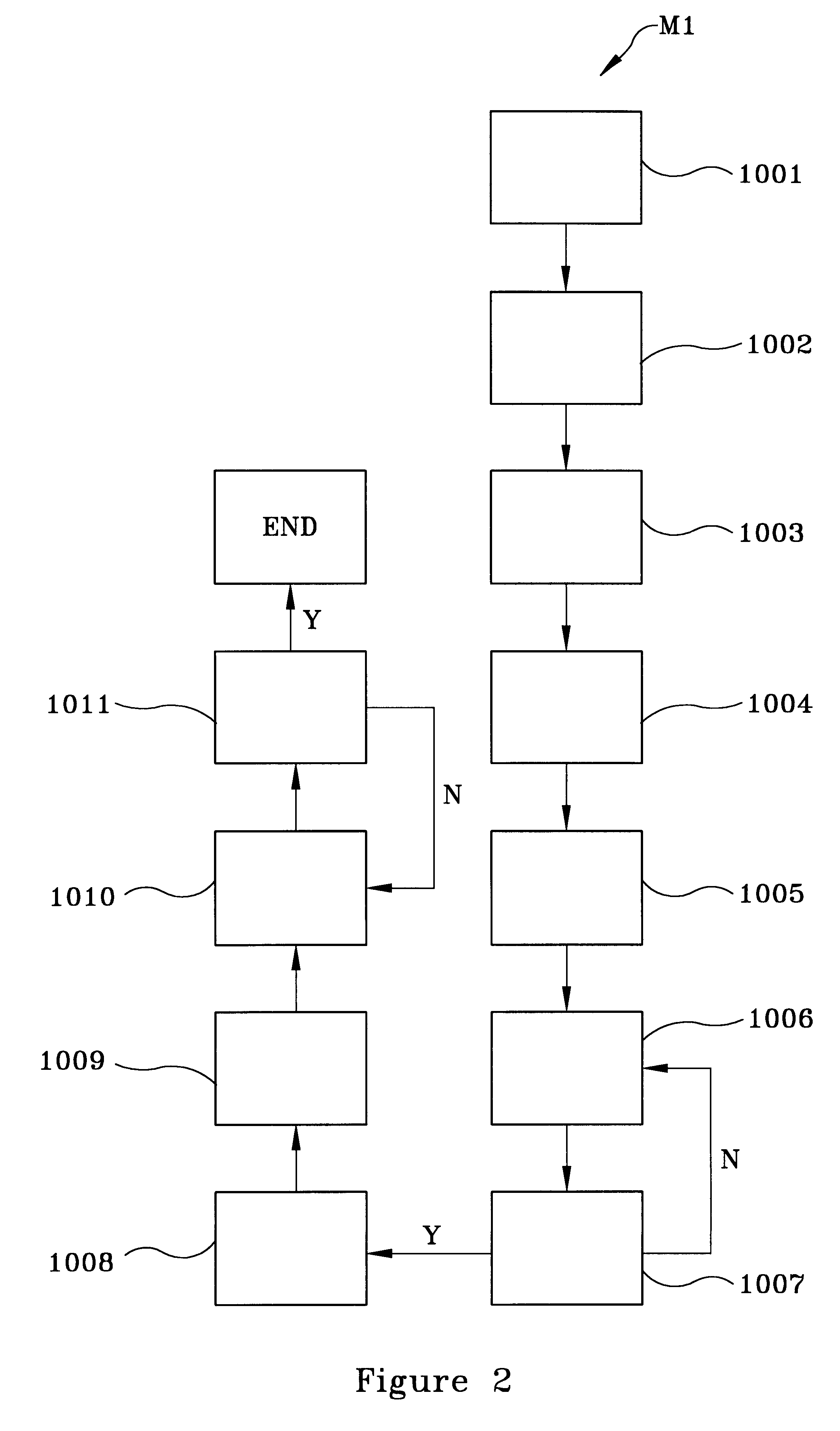
FIG. 2 flowcharts, by example only, a method M1 of synthesizing a liter of a unique nontoxic aqueous Cu--Zn electroplating (chemical) solution, in accordance with the present invention:

(1) cleaning a mixing vessel (e.g., a beaker) with dilute nitric acid (HNO.sub.3) for approximately 5 minutes, as indicated by block 1001;

(2) rinsing the mixing vessel in deionized (DI) water for approximately 5 minutes to approximately 10 minutes and subsequently drying the mixing vessel, for instance, under a gaseous nitrogen (GN.sub.2) flow, as indicated by block 1002;

(3) adding an initial volume of DI water (e.g., approximately 400 ml) to the mixing vessel, as indicated by block 1003;

(4) adding at least one Cu ion source for providing a plurality of Cu ions and stirring the at least one Cu ion source into the DI water for a dura...


PUM

PropertyMeasurementUnit
Currentaaaaaaaaaa
Currentaaaaaaaaaa
Electric potential / voltageaaaaaaaaaa

Abstract

A method of fabricating a semiconductor device, having a Cu-rich Cu-Zn alloy thin film (30) formed on a cathode-wafer such as a Cu surface (20) by electroplating, using an electroplating apparatus, the Cu surface (20) in a unique chemical solution containing salts of zinc (Zn) and copper (Cu), their complexing agents, a pH adjuster, and surfactants; and a semiconductor device thereby formed. The method controls the parameters of pH, temperature, and time in order to form a uniform Cu-rich Cu-Zn alloy thin film (30) for reducing electromigration on the cathode-wafer by decreasing the drift velocity therein which decreases the Cu migration rate in addition to decreasing the void formation rate, for improving device reliability, and for increasing corrosion resistance.

Description

The present invention relates to semiconductor devices and their methods of fabrication. More particularly, the present invention relates to the processing of copper interconnect material and the resultant device utilizing the same. Even more particularly, the present invention relates to reducing electromigration in copper interconnect lines by doping their surfaces with a barrier material using wet chemical methods.Currently, the semiconductor industry is demanding faster and denser devices (e.g., 0.05-.mu.m to 0.25-.mu.m) which implies an ongoing need for low resistance metallization. Such need has sparked research into resistance reduction through the use of barrier metals, stacks, and refractory metals. Despite aluminum's (Al) adequate resistance, other Al properties render it less desirable as a candidate for these higher density devices, especially with respect to its deposition into plug regions having a high aspect ratio cross-sectional area. Thus, research into the use of ...

Claims


Application Information

Patent Timeline
IPC IPC(8): C25D5/18C25D7/12C25D3/56C25D5/00C25D3/58H01L21/02H01L21/768H01L21/70H01L21/288
CPCC25D3/58C25D5/18H01L21/2885H01L21/7685C25D7/12C25D17/001C25D5/617C25D7/123
Inventor LOPATIN, SERGEYNICKEL, ALEXANDER H.
Owner ADVANCED MICRO DEVICES INC
Why Eureka
Try Eureka