Gate drive for insulated gate power semiconductors

a gate drive and power semiconductor technology, applied in the direction of electronic switching, power conversion systems, pulse techniques, etc., can solve the problems of significant change in magnetic flux, circuitry production, and difficult to meet the trade-off between electromagnetic interference (emi) and power loss, and achieve large concurrent improvements in both switching losses and emi, easily and individually controlled

Inactive Publication Date: 2003-04-29
WALLACE GREGORY CRAIG MR
View PDF13 Cites 17 Cited by
  • Summary
  • Abstract
  • Description
  • Claims
  • Application Information

AI Technical Summary

Benefits of technology

The representations shown in FIG. 7 of the invention provide a mechanism to independently and continuously control the slope of both the drain voltage and drain current waveforms during both the turn-on and turn-off processes of insulating gate power devices. This allows very large concurrent improvements in both switching losses and EMI. The four parameters of turn-on current, turn-off current, turn-on voltage and turn-off voltage can be easily and individually controlled through the use of variable resistors VR1, VR2, VR3 and VR4 (as shown on FIGS. 7 and 8) respectively. The drain current control could alternatively be controlled by indirectly changing the value of the current sources through variable voltages.
However, independent of the embodiment of the control of these parameters, it is possible to have all four parameters mentioned above indirectly under software or firmware control from a micro-controlle

Problems solved by technology

However, the switching trajectories for both types of devices are responsible for both common-mode electromagnetic emissions generated by the drain current waveform and power losses in the commutation cell.
As requirements of miniaturisation drive the switching frequencies higher, a satisfactory trade off between electromagnetic interference (EMI) and power losses becomes increasingly difficult.
This waveform produces E-field radiation and common mode conducted interference which is caused by parasitic capacitances to ground returns.
However the similarity of the rectangular switching currents in the commutation circuitry produces significant changing magnetic flux.
This induces high frequency noise throughout the circuit, resulting in H-field radiation and interferenc

Method used


Image

  • Gate drive for insulated gate power semiconductors
  • Gate drive for insulated gate power semiconductors
  • Gate drive for insulated gate power semiconductors

Examples


example 2

EMI Improvement for Turn-on

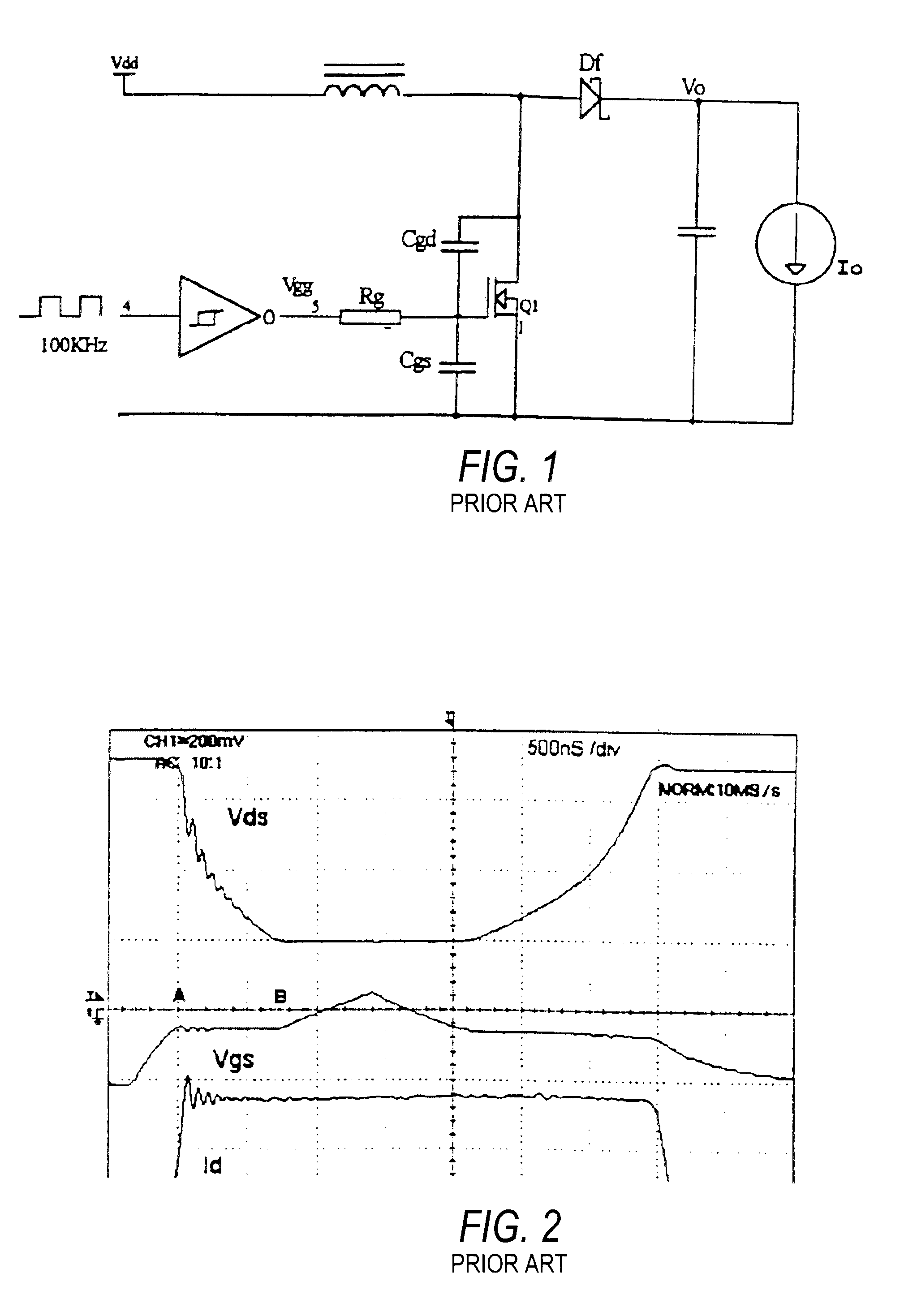
Referring to FIG. 6, a graphical representation of the near-field radiated emissions of the known driver (FIG. 1) and of the circuitry of the preferred embodiment, are thereshown for the same voltage switching times. The parameters are as set out below in Table 2.

FIG. 6 graphs the frequency spectrum obtained using an EMC analyser. The graph for the known, conventional driver is the line 61 and graph of the driver in accordance with the present invention is the line 62. The full improvement cannot be seen as the emission level from the invention reaches the noise floor of the measuring equipment before the conventional drive.

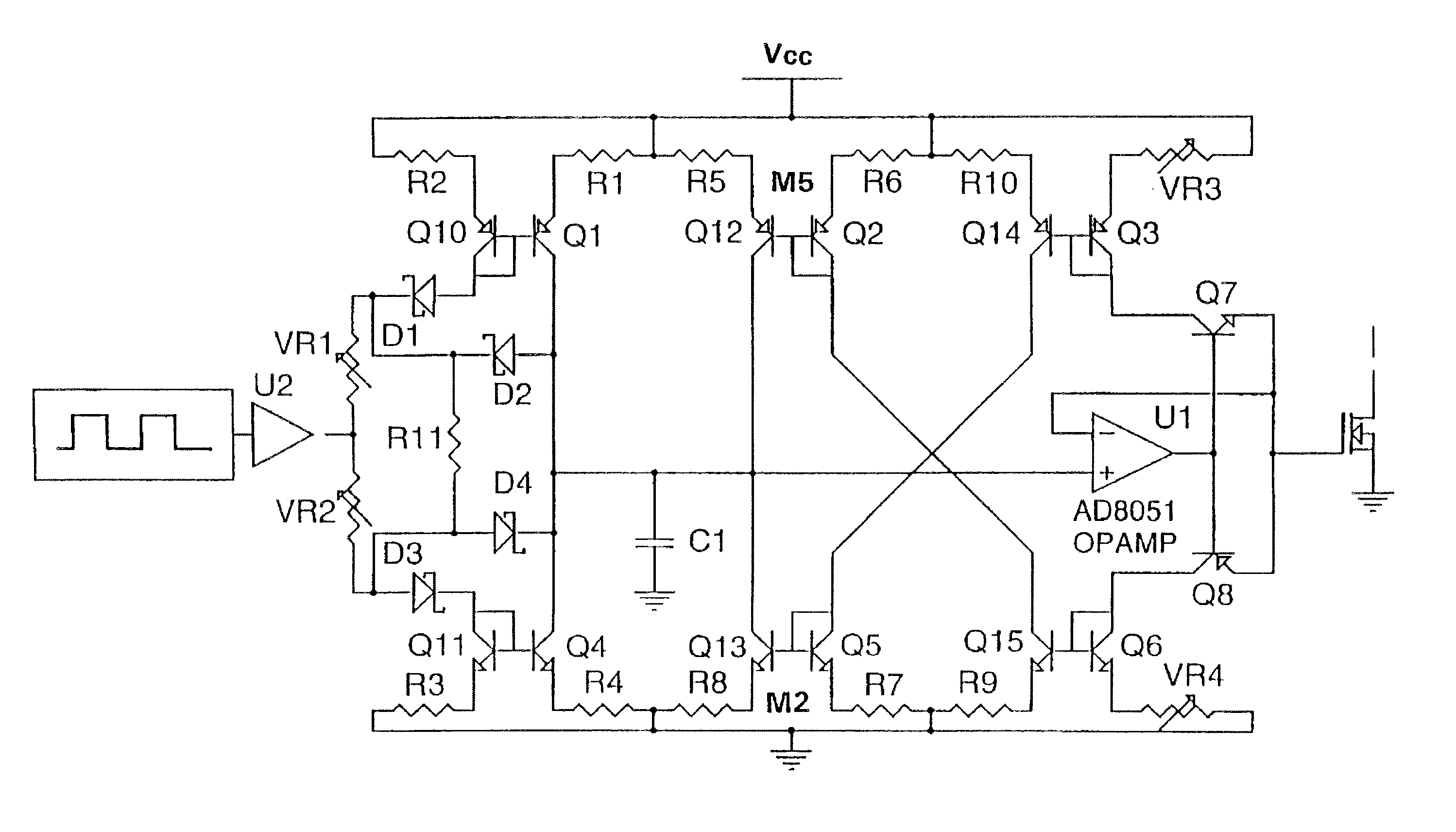
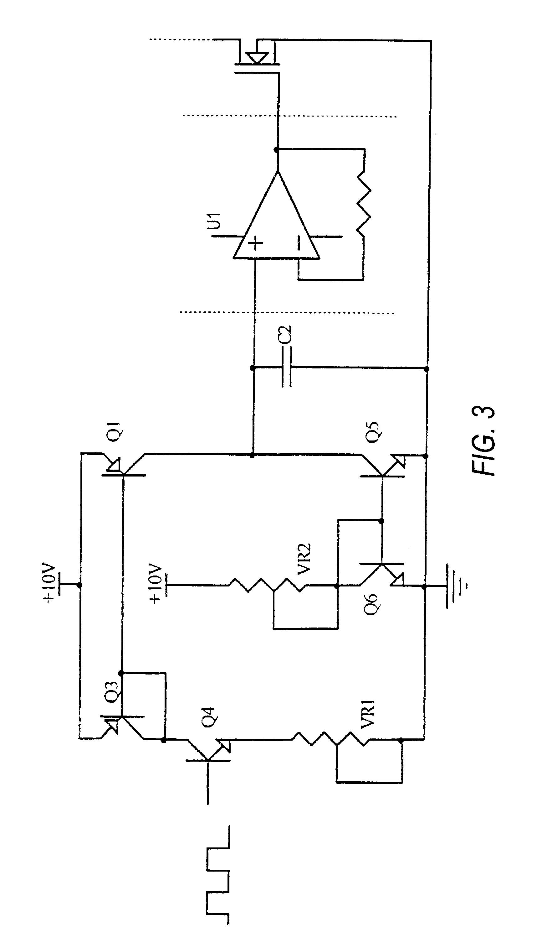
The above describes a preferred embodiment of the circuit for switch-on and is applicable to both MOSFETs and IGBTs.

Turn-Off

The circuit of FIG. 4 achieves similar improvements during turn-off as those shown for turn-on.

This applies fully to MOSFETs, but only to IGBTs during the miller effect and power mos phases. The dv.sub.ds / dt can b...


PUM


Abstract

A method of control of the current and voltage switching trajectories of insulated gate power semiconductor switches, more specifically MOSFETs and insulated gate bipolar transistor devices (IGBTs), is disclosed. MOSFETs and IGBTs are used in switch mode power supplies because of their easy driving ability and their ability to handle high currents and voltages at high-switching frequencies. However, the switching trajectories for both types of devices are responsible for both common-mode electromagnetic emissions generated by the drain current waveform and power losses in the commutation cell. These two characteristics represent opposing design objectives for power converters. The current invention uses a hybrid voltage/current gate signal source with feedback of the gate charge (or discharge) current to dynamically and independently control the drain current and drain voltage of an insulated semiconductor device. The rate of change of drain current is controlled by the voltage source traversing the transconductance curve while the rate of change of the drain voltage is controlled by dynamic variations in the current source due to feedback.

Description

The present invention relates to an analogue gate drive for insulated gate power semiconductors. More specifically it relates to control of the current and voltage switching trajectories of insulated gate power semiconductor switches, which has application in the area of fundamental power electronics.MOSFETs and insulated gate bipolar transistor devices (IGBTs) are used in switch mode power supplies (SMPS) because of their easy driving ability and their ability to handle high currents and voltages at high-switching frequencies.However, the switching trajectories for both types of devices are responsible for both common-mode electromagnetic emissions generated by the drain current waveform and power losses in the commutation cell. These two characteristics represent opposing design objectives for power converters. As requirements of miniaturisation drive the switching frequencies higher, a satisfactory trade off between electromagnetic interference (EMI) and power losses becomes incr...

Claims


Application Information

Patent Timeline
IPC IPC(8): H03K17/16H03K17/687H03K4/00
CPCH03K4/00H03K17/6877H03K17/163H02M1/08
Inventor WALLACE, GREGORY CRAIG
Owner WALLACE GREGORY CRAIG MR
Why Eureka
Try Eureka