Method of patterning magnetic products using chemical reactions

a magnetic product and chemical reaction technology, applied in the field of high-density magnetic recording technology, can solve the problems of reducing the quantity of magnetization per bit, limiting the resistance to thermal fluctuation, and loss of magnetization information, and achieve the effect of high integration

Inactive Publication Date: 2005-01-11
KK TOSHIBA
View PDF14 Cites 63 Cited by
  • Summary
  • Abstract
  • Description
  • Claims
  • Application Information

AI Technical Summary

Benefits of technology

[0029]An object of the present invention is to provide a magnetic material patterning method applicable to manufacturing of various magnetic products, which causes no physical damage and has high productivity.
[0032]According to the first aspect invention, since the nonferromagnetic material layer is selectively formed by the chemical reaction between halogen and the ferromagnetic material layer, a magnetic pattern composed of ferromagnetic and nonferromagnetic material layers can be formed. Because of the use of the chemical reaction, no physical damage is incurred, and also a large region can be patterned in a batch process. The halogenated nonferromagnetic material region has little volume expansion different from the case of oxidation, and thus an extremely smooth surface can be obtained without a step of polishing the surface. Moreover, because of the use of halogenation reaction, a general resist can be used, and oxygen ashing process can be used for removing the resist. By using this magnetic material patterning, it is possible to manufacture patterned medium, to write servo information in a magnetic recording medium all at once, and to manufacture various magnetic products including a magnetic recording element such as an MRAM, and the like.
[0034]According to the second aspect, a patterned medium is provided by the recording region made of the ferromagnetic material and the nonferromagnetic material region made of the halogen compound of this ferromagnetic material. Since this nonferromagnetic material region is formed by the chemical method, the recording region is not damaged. Accordingly, manufacturing conditions cause no deterioration of magnetic properties, and good magnetic properties can be obtained. In addition, the surface of the nonferromagnetic material region and the recording region is not uneven, and a magnetic recording medium having high substrate smoothness can be provided.
[0036]According to the third aspect, since servo information to be written in the servo layer of the magnetic recording medium is written based on a pattern of presence / non-presence of a halogen compound layer which can be formed by chemical reaction. Therefore the servo information can be written in a large area all at once. Moreover, if the servo information is written based on the presence / non-presence of the halogen compound layer, since volume expansion of the halogen compound layer is very small, a magnetic recording medium having excellent smoothness of a substrate surface can be provided.
[0038]According to the fourth aspect, the insulating layer surrounding the first ferromagnetic material layer, the tunnel insulating layer, and the second ferromagnetic material layer is formed of a halogen compound layer. Therefore element formation can be carried out by employing a magnetic material patterning method using halogenation reaction accompanied with no etching. Thus, no leakage due to etching is incurred, and an MRAM having high integration can be provided in a large-area batch process.

Problems solved by technology

However, the minute recording bit reduces a quantity of magnetization per bit, and there arises a problem that is loss of magnetization information due to magnetization reversal by “thermal fluctuation”.
However, if a density of the HDD is increased much more in the future, there may be a limit to resistance to thermal fluctuation even for the perpendicular magnetic recording mode.
However, since the magnetic material is hard to be etched unlike a general semiconductor material, it is difficult to use normal reactive ion etching (RIE) used in a semiconductor process.
However, in the above-described conventional manufacturing method, since the ferromagnetic material layer 520 is fabricated using the ion beam milling, damage remains on a crystal structure of the fabricated surface.
Thus, to carry out fabrication of a good aspect ratio, a thin resist cannot be used.
However, there is a level difference of 20 to 50 nm attributable to presence / non-presence of a magnetic layer on the medium surface, and the level difference causes a problem of considerably reducing seeking durability.
However, these methods cannot completely remove the level difference on the medium surface.
Consequently, the removing the mask material brings a process load.
However, short-circuiting may occur between the upper and lower ferromagnetic material layers because of etching damage or etching residuals.
On the other hand, the following problems exist concerning writing in the servo region formed in the magnetic recording medium.

Method used


Image

  • Method of patterning magnetic products using chemical reactions
  • Method of patterning magnetic products using chemical reactions
  • Method of patterning magnetic products using chemical reactions

Examples


example 1

[0086]First, CoPt was deposited by 20 nm on a Si substrate by a sputtering method, and a magnetic force microscope (MFM) image on a surface of this sample was observed. An image of a perpendicular magnetic recording medium having a high-contrast maze pattern which is a typical ferromagnetic pattern was observed. A hysteresis curve in a perpendicular direction was measured by a vibrating sample magnetometer (VSM), and a curve, as shown in FIG. 4A, which has a squareness ratio of 0.49 and a coercive force of 1500 Oe was obtained.

[0087]Then, a composition of the sample surface was analyzed by using X-ray photoelectron spectroscopy (XPS). A peak inherent in Co was observed at binding energy=778 eV. A peak (781 eV) of CoO was simultaneously observed; however, this peak was due to natural oxidation of oxygen in the atmosphere. Two peaks inherent in Pt were also observed within the range from 70 to 75 eV.

[0088]Subsequently, CoPt was deposited by 20 nm on the Si substrate by the sputtering ...

example 2

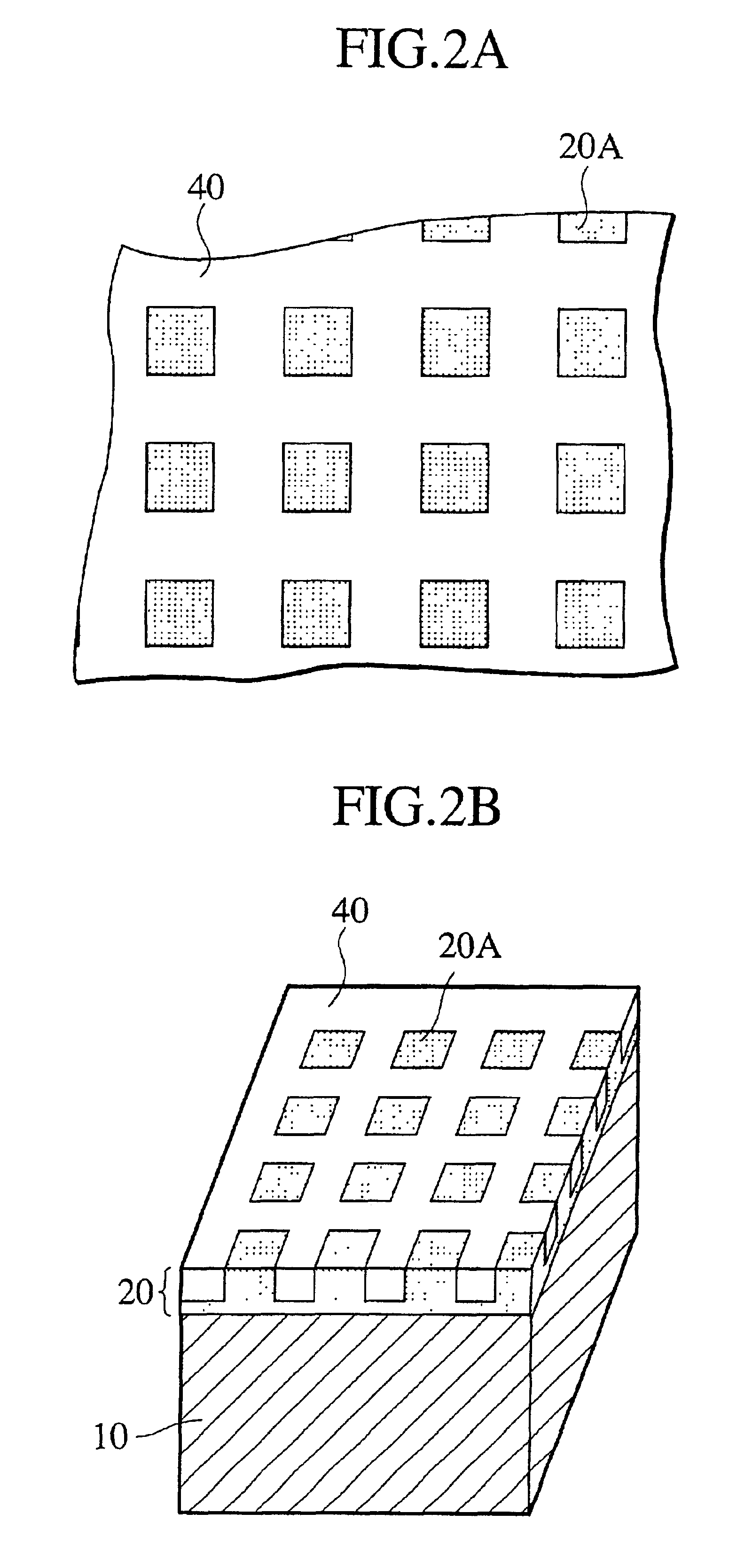
[0094]A patterned medium sample, in which ferromagnetic material CoPt regions are surrounded by antiferromagnetic material CoF2, was prepared. That is, first, CoPt was deposited by 20 nm on a Si substrate by a sputtering method. Then, resist was coated in a thickness of about 1.0 μm on this CoPt film by spin coating, and a resist pattern as shown in FIG. 5A was formed after batch exposure and development. In this example, a size of each ferromagnetic material region on a surface layer was set to 2.0 μm square.

[0095]A surface of this sample was exposed in F radicals generated under conditions similar to those of the example 1 for about 30 seconds while being maintained at room temperature. Then, the resist was removed by using an oxygen ashing apparatus.

[0096]When a MFM image of this sample was observed, a magnetic pattern equivalent to a resist pattern as shown in FIG. 5B was obtained. That is, regarding a region covered with a resist film, a MFM image of a ferromagnetic material ha...

example 3

[0099]In order to form finer patterns of the ferromagnetic material region than that of the above-described example 2, electron beam (EB) writing was carried out in exposure of resist. Accordingly, fine ferromagnetic material region patterns of about 80 nm square were formed. Other conditions were the same as those of the above example 2, and by using these conditions, a sample was prepared. That is, CoPt was deposited by 20 nm on a Si substrate by sputtering. Then, nega-resist was coated thereon, a minute resist pattern was formed by EB writing, and exposure thereof in F radicals was carried out for about 30 seconds at room temperature. Thereafter, the resist was removed.

[0100]An obtained sample was observed by MFM, and a single color image was obtained in a ferromagnetic material region. That is, it was verified that by reducing the ferromagnetic material region to a size of about 80 nm square, a single magnetic domain state was set in this region. When magnetic properties in a pe...


PUM

PropertyMeasurementUnit
depthaaaaaaaaaa
thicknessaaaaaaaaaa
Neel temperaturesaaaaaaaaaa

Abstract

A method of patterning magnetic material includes forming a ferromagnetic material layer containing one element selected from the group consisting of Fe, Co and Ni on a substrate, selectively masking a surface of the ferromagnetic material layer, and making nonferromagnetic. The making nonferromagnetic step includes exposing an exposed portion in halogen-containing reaction gas, changing magnetism of the exposed portion and a lower layer thereof by chemical reaction, and making the exposed portion a nonferromagnetic material region. A magnetic recording medium is fabricated by using the magnetic material patterning method and includes a plurality of recording regions made of ferromagnetic materials, each containing at least one element selected from the group consisting of Fe, Co and Ni, and a nonferromagnetic material region for separating the recording regions from each other. The nonferromagnetic material region is a compound region of the ferromagnetic material and halogen.

Description

CROSS REFERENCE TO RELATED APPLICATION[0002]This application is based upon and claims the benefit of priority from the prior Japanese Patent Applications No. 2001-102215 filed on Mar. 30, 2001 and No. 2001-399848 filed on Dec. 28, 2001, the entire contents of which are incorporated herein by reference.BACKGROUND OF THE INVENTION[0003]1. Field of the Invention[0004]The present invention relates to a high-density magnetic recording technology and, more particularly, to a method of patterning magnetic products, magnetic recording media such as patterned media produced by this method, and other magnetic products, and to a magnetic recording apparatus equipped with such magnetic recording media.[0005]2. Description of the Related Art[0006]In recent years, because of an increase in a surface recording density of a magnetic recording medium along with an increased recording capacity of a hard disk drive (referred to as HDD, hereinafter), each recording bit size on the magnetic recording me...

Claims


Application Information

Patent Timeline
Patent Type & Authority Patents(United States)
IPC IPC(8): G11B5/855G11B5/00G11B5/48G11B5/74G11B9/00G11B5/64G11B5/58G11B5/596G11B5/65G11B5/82G11B5/84H01F10/16H01F41/34H01L21/8246H01L27/105H01L43/08
CPCB82Y10/00G11B5/74G11B5/743G11B5/82G11B5/855G11B5/00Y10T428/12465G11B5/488G11B5/58G11B5/596G11B9/1418G11B2005/0002G11B2005/0005Y10T428/31Y10T428/24479Y10T428/25H10N50/01
Inventor KAMATA, YOSHIYUKINAITO, KATSUYUKIHIEDA, HIROYUKI
Owner KK TOSHIBA
Why Eureka
Try Eureka