Semiconductor device and method of fabricating the same
- Summary
- Abstract
- Description
- Claims
- Application Information
AI Technical Summary
Benefits of technology
Problems solved by technology
Method used
Image

Examples
first embodiment
Next, a process of creating a self-aligned contact (SAC) hole in the present invention will be described with reference to FIGS. 3A to 3C.
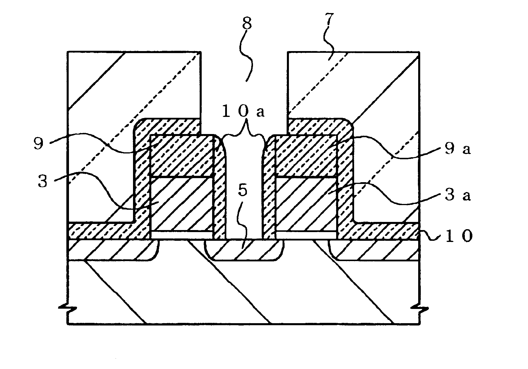
As illustrated in FIG. 3A, gate insulating films 2, 2a made of silicon oxynitride films of approximately 4 nm thick are formed on the surface of silicon substrate 1, and gate electrodes 3, 3a are formed respectively on gate insulating films 2, 2a, in a manner similar to the counterparts described in connection with FIGS. 2A to 2C. Here, gate electrodes 3, 3a are in a so-called tungsten polyside structure as comprised of a WSi (tungsten silicide) layer and a polycrystalline silicon layer, which has a thickness and a pattern width of 150 nm, by way of example. Then, protective insulating layers 4, 4a are formed on gate electrodes 3, 3a, respectively. Here, protective insulating layers 4, 4a are first silicon nitride films of 100 nm thick. Then, source / drain diffusion layers 5, 5a are formed. Gate electrodes 3, 3a are spaced by 150 nm from each other...
second embodiment
Next, a process of manufacturing a self-aligned contact hole in the present invention will be described with reference to FIGS. 5A to 5C. In FIGS. 5A to 5C, components identical to those in FIGS. 3A to 3C are designated the same reference numerals.
Similarly, in the second embodiment as illustrated in FIG. 5A, gate insulating films 2, 2a and gate electrodes 3, 3a are also formed on the surface of silicon substrate 1, and protective insulating layers 9, 9a are formed respectively on gate electrodes 3, 3a. Here, protective insulating layers 9, 9a are first silicon carbide films of 100 nm thick. Then, source / drain diffusion layers 5, 5a are formed. Gate electrodes 3, 3a are spaced by 150 nm from each other. The silicon carbide films constituting protective insulating layers 9, 9a are deposited by a plasma CVD method using trimethylsilane (SiH(CH3)3) as a reactant gas. The silicon carbide film formed in this manner has the insulating property and a dielectric constant equal to 4.6 which ...
third embodiment
Next, the present invention will be described with reference to FIGS. 7A to 7E. In the third embodiment, a contact hole is formed in a self-aligned manner with a wiring layer such as bit lines which are disposed in parallel.
As illustrated in FIG. 7A, diffusion layers 12, 12a of N-conductivity type are formed on the surface of silicon substrate 11 of P-conductivity type by ion implantation and thermal treatment. Then, first interlayer insulating film 13 is formed in thickness of approximately 500 nm. First interlayer insulating film 13 is fabricated by depositing a silicon oxide film by a plasma CVD method, and subsequently planarizing the silicon oxide film by a CMP method.
A tungsten (W) film or a laminate film comprised of W and tungsten nitride (WN) of 50 nm thick is deposited on planarized first interlayer insulating film 13 by a CVD method or a sputtering method. Then, a protective insulating layer is formed by a thermal CVD method. Here, the protective insulating layer is a sil...
PUM
 Abstract
Description
Claims
Application Information
 - Generate Ideas
- Intellectual Property
- Life Sciences
- Materials
- Tech Scout
- Unparalleled Data Quality
- Higher Quality Content
- 60% Fewer Hallucinations
Browse by: Latest US Patents, China's latest patents, Technical Efficacy Thesaurus, Application Domain, Technology Topic, Popular Technical Reports.
© 2025 PatSnap. All rights reserved.Legal|Privacy policy|Modern Slavery Act Transparency Statement|Sitemap|About US| Contact US: help@patsnap.com