

High power deep ultraviolet laser with long life optics
- Summary
- Abstract
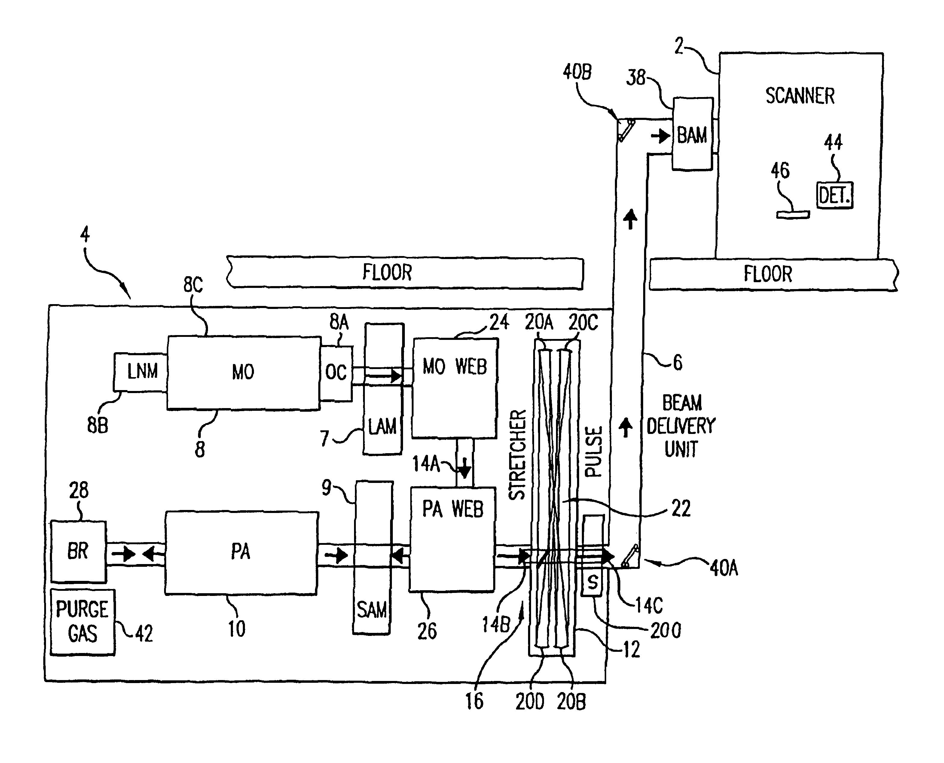
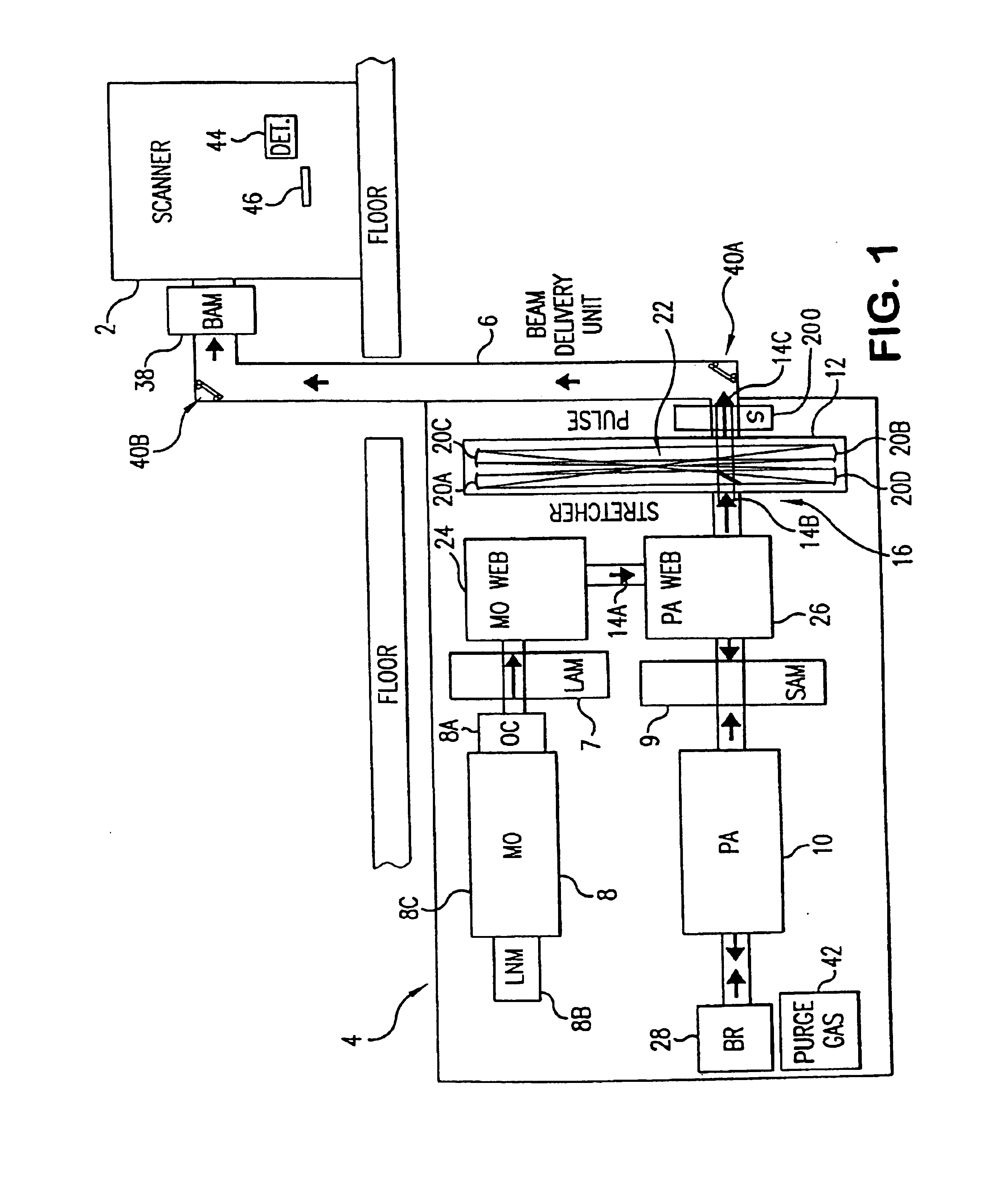
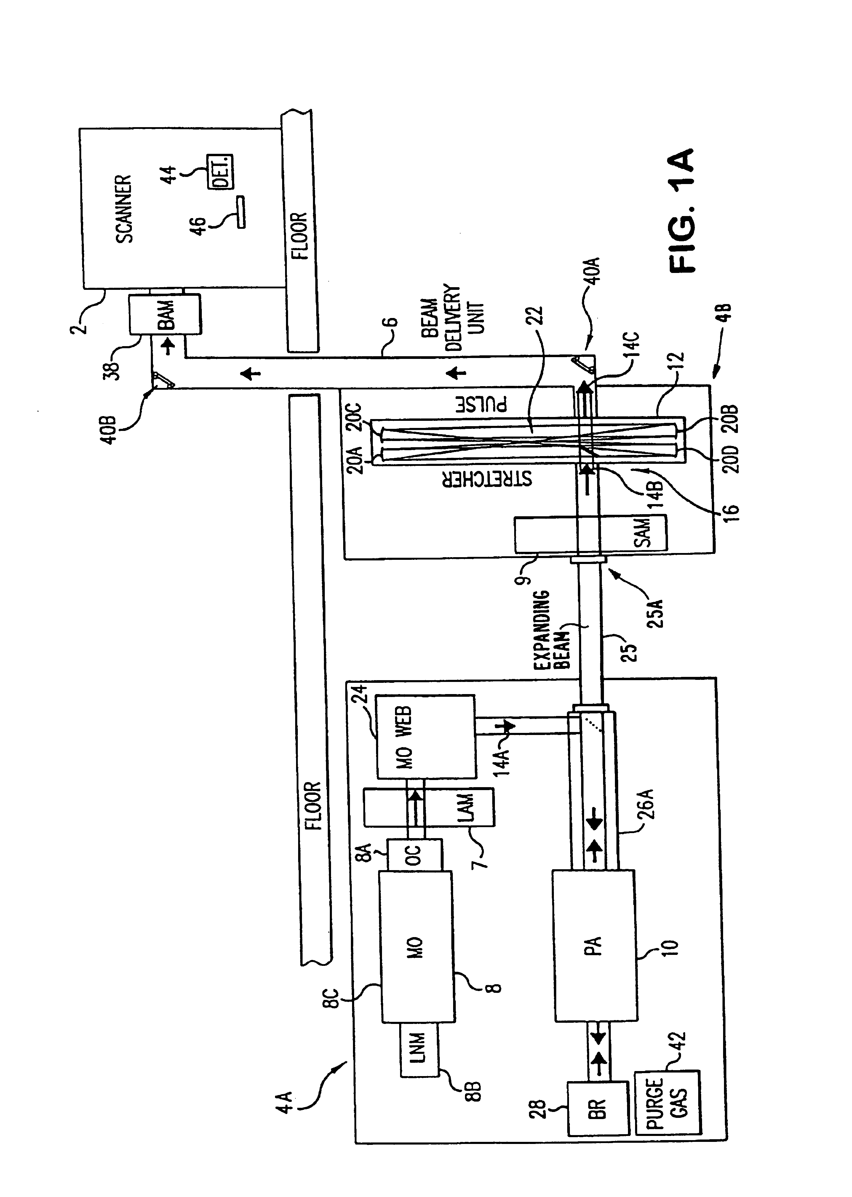
- Description
- Claims
- Application Information
AI Technical Summary
Benefits of technology
Problems solved by technology
Method used
Image

Examples
Embodiment Construction
CAF2 Optical Surface Damage
Discovery of Surface Damage Problem
[0055]Applicants' testing with ArF MOPA systems described herein has revealed that prior art CaF2 optics can suffer severe surface degradation when subjected to 20 ns pulses of 193 nm ultraviolet radiation at the average pulse fluence levels in the range of about 44 mJ / cm2 to about 130 mJ / cm2. The damage occurs at both the beam entrance surface and the exit surface even when the optics are purged with high quality purge gases such as nitrogen and helium. With 20 ns pulses and with average fluences below 20 mJ / cm2 and with a good purge, the CaF2 optics performs very well for billions of pulses. In the range between 20 mJ / cm2 to 100 mJ / cm2 lifetime is uncertain and hard to predict. At fluences greater than 100 mJ severe damage to the surfaces of the optics occurs almost immediately. Applicants discovered to their surprise that no damage occurs on the inside surface of the laser chamber output window at high pulse fluences i...
PUM
 Abstract
Description
Claims
Application Information