Flexible printed wiring board for chip-on flexibles

a flexible, printed technology, applied in the direction of metallic pattern materials, metallic resin layered products, metallic material coating processes, etc., can solve the problems of not being able to identify the surface shape affecting the scattering of light, and be difficult to secure adhesion, improve adhesion, and improve adhesion

Inactive Publication Date: 2006-01-10
MITSUI MINING & SMELTING CO LTD
View PDF8 Cites 23 Cited by
  • Summary
  • Abstract
  • Description
  • Claims
  • Application Information

AI Technical Summary

Benefits of technology

[0025]As described above, in the flexible printed wiring board according to the present invention, although a polyimide-based resin is often used as the insulating layer, the adhesion between the insulating layer composed of such a polyimide-based resin and the electrodeposited copper foil is not so good, and it is said that the adhesion strength (peeling strength) is difficult to secure. In particular, when an electrodeposited copper foil is directly adhered to a film or a base material consisting of a polyimide-based resin without using an adhesive or the like, the adhesion is much worsened. However, when the rust proofing layer is formed of a nickel-zinc alloy, and an amino functional silane coupling agent adsorbed layer is further formed, the adhesion strength to the insulating layer consisting of a polyimide-based resin can be maintained at a certain level.
[0026]When a resin agent is applied, for example, ...

Problems solved by technology

Therefore, it could not be said to be sufficient to i...

Method used


Image

  • Flexible printed wiring board for chip-on flexibles
  • Flexible printed wiring board for chip-on flexibles
  • Flexible printed wiring board for chip-on flexibles

Examples


first embodiment

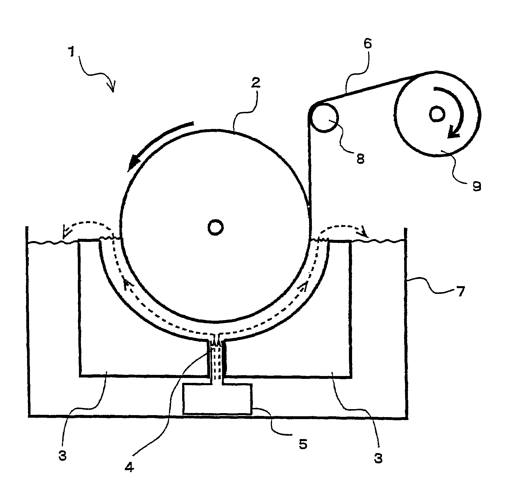
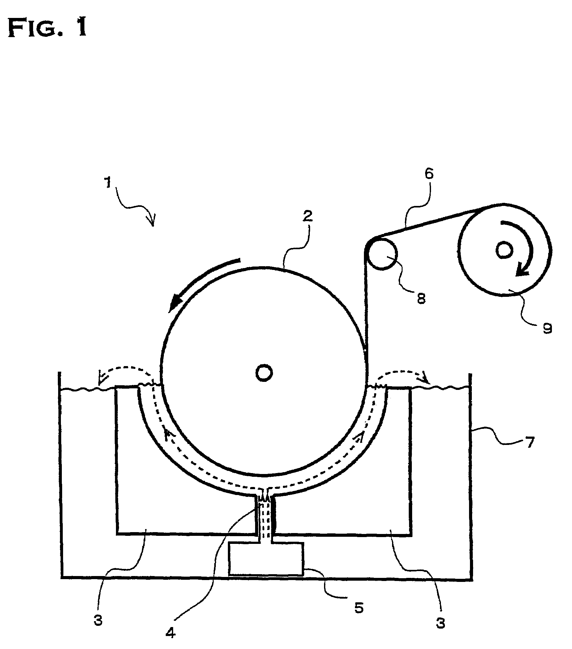
[0034]First, in the first embodiment, the manufacture of an electrodeposited copper foil used in the flexible printed wiring board of the present invention will be described. The electrodeposited copper foil is manufactured with electrodeposited copper foil manufacturing equipment using a conventionally known rotating drum cathode, and the schematic sectional view is shown in FIG. 1. The electrodeposited copper foil manufacturing equipment 1 is equipped with a rotating drum cathode 2 made of titanium (diameter: 3 m; width: 1.35 m) for electrodepositing copper, and an insoluble anode 3 known as DSA placed opposite along the peripheral surface shape of the rotating cathode 2. The rotating cathode 2 and the anode 3 are connected to a power supply unit (not shown). The rotating drum cathode 2 is designed so that a substantially half of the volume is immersed in an electrolyte solution; the anode 3 is divided into two portions, and an electrolyte supply means 5 having an electrolyte supp...

second embodiment

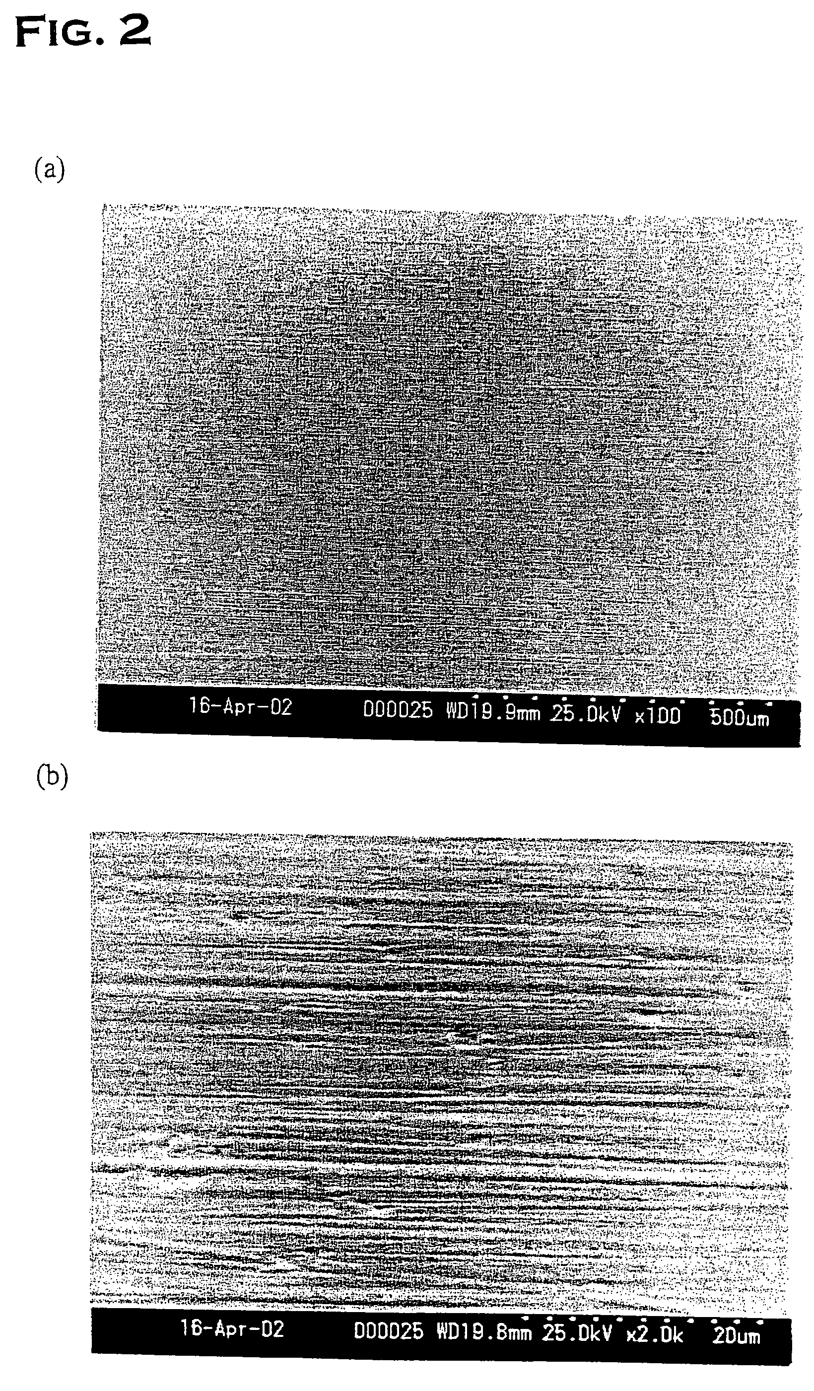
[0048]In the second embodiment, the results of examinations about the specular gloss and the optical transmittance of the adhering surface of an electrodeposited copper foil characterized by the types and the surface treatment thereof, particularly with or without nodular treatment, will be described. Table 5 shows various electrodeposited copper foils, and the results of the specular gloss and the optical transmittance thereof.

[0049]

TABLE 5Adhering surfaceSpecular glossRoughenedRoughnessIncident angle 60°OpticalConductive layertreatmentRz μmMDTDtransmittance %ComparativeNormal foil matteYes4.51.31.11.1Example A-1surfaceComparativeMatte side of low-Yes3.51.01.00.8Example A-2roughness foilComparativeShiny side of low-Yes2.60.10.23.7Example A-3roughness foilComparativeShiny side of low-Yes1.70.30.831.3Example A-4roughness foilComparativeShiny side of low-No1.674.8100.644.9Example A-5roughness foilComparativeVacuum-deposited + copper-No———75.0Example A-6plated foilExample A-1Foil of th...

third embodiment

[0055]Finally, concerning the rust proofing treatment on the adhering surface of electrodeposited copper foils, the results of examining the adhesion and migration resistance when flexible printed wiring boards were constituted will be described.

[0056]Adhesion study in the third embodiment was conducted using the electrodeposited copper foil prepared in the same manner as in Example 3 of the above-described first embodiment, whereto each rust proofing treatment shown in Table 6 was performed.

[0057]

TABLE 6Surface treatment of adhering surfaceEvaluationRust proofing treatmentPealing strengthAdhering(kgf / cm)quantitySilane coupling agentIn normalAfterOpticalKindmg / m2TypeConcentrationstateheatingBlackeningtransmittance (%)ComparativeZn36.3a50.380.27Good73.1Example B-1ComparativeZn36.3b50.24—Good68.4Example B-2ComparativeZn36.3c50.00—Good69.2Example B-3ComparativeZn36.3d50.10—Good71.5Example B-4ComparativeZn36.3e50.410.24Good70.3Example B-5ComparativeSn33.0a50.440.68No good51.5Example B-6...


PUM

PropertyMeasurementUnit
Angleaaaaaaaaaa
Lengthaaaaaaaaaa
Fractionaaaaaaaaaa

Abstract

There is provided a flexible printed wiring board including an insulating layer having a high optical transmittance, a high adhesion strength and a high migration resistance, and suitable for a chip on film (hereafter referred to as COF). In a flexible printed wiring board for COF, having an insulating layer on which a conductive layer of an electrodeposited copper foil is laminated, and an optical transmittance of 50% or more of the insulating layer in the etched region when a circuit is formed by etching said conductive layer, electrodeposited copper foil was made to have a rust-proofing layer of a nickel-zinc alloy on the adhering surface to be adhered to the insulating layer; the surface roughness (Rz) of the adhering surface was made to be 0.05 to 1.5 μm, and the specular gloss was made to be 250 or more when the incident angle is 60°.

Description

CROSS REFERENCE TO RELATED APPLICATION[0001]This application is a 35 USC § 371 National Phase Entry Application from PCT / JP03 / 05891, filed May 12, 2003, and designating the U.S.TECHNICAL FIELD[0002]The present invention relates to a flexible printed wiring board, and specifically to a flexible printed wiring board suitable for a chip-on-film type.BACKGROUND ART[0003]In recent years, accompanying the progress of the electronic device industry, demands for flexible printed wiring boards for mounting electronic parts such as ICs and LSIs have rapidly increased. Thus, the down sizing, that is, the size and weight reduction, and functional enhancement of electronic devices themselves have markedly progressed. For this purpose, packaging systems using flexible film carrier tapes, such as TAB (tape automated bonding) tapes, T-BGA (ball grid array) tapes, and ASIC (application specific integrated circuit) tapes, have been adopted. Particularly, in electronic devices having Liquid crystal di...

Claims


Application Information

Patent Timeline
IPC IPC(8): B21D39/00C23C26/00C23C28/00C23C30/00C25D1/04C25D3/56C25D5/48H05K1/00H05K3/38
CPCC23C26/00C23C28/321C23C30/00C25D1/04C25D3/562C25D5/48H05K3/384C23C28/3455C23C28/00Y10T428/12514H05K1/0393H05K3/389H05K2201/0355H05K2203/0723Y10T428/12792Y10T428/12993Y10T428/12472Y10T428/2804Y10T428/12903Y10T428/12535Y10T428/12569Y10T428/2843H05K1/09
Inventor OKADA, KAZUYUKIHARA, YASUJIUCHIYAMA, AKIRATAKAHASHI, MASARU
Owner MITSUI MINING & SMELTING CO LTD
Why Eureka
Try Eureka