

Semiconductor device structure
a technology of semiconductor devices and semiconductor devices, applied in semiconductor devices, electrical equipment, instruments, etc., can solve the problems of inability to use tfts, no prospect of mass production, and the method is not free from problems
- Summary
- Abstract
- Description
- Claims
- Application Information
AI Technical Summary
Benefits of technology
Problems solved by technology
Method used
Image

Examples
embodiment 1
[Embodiment 1]
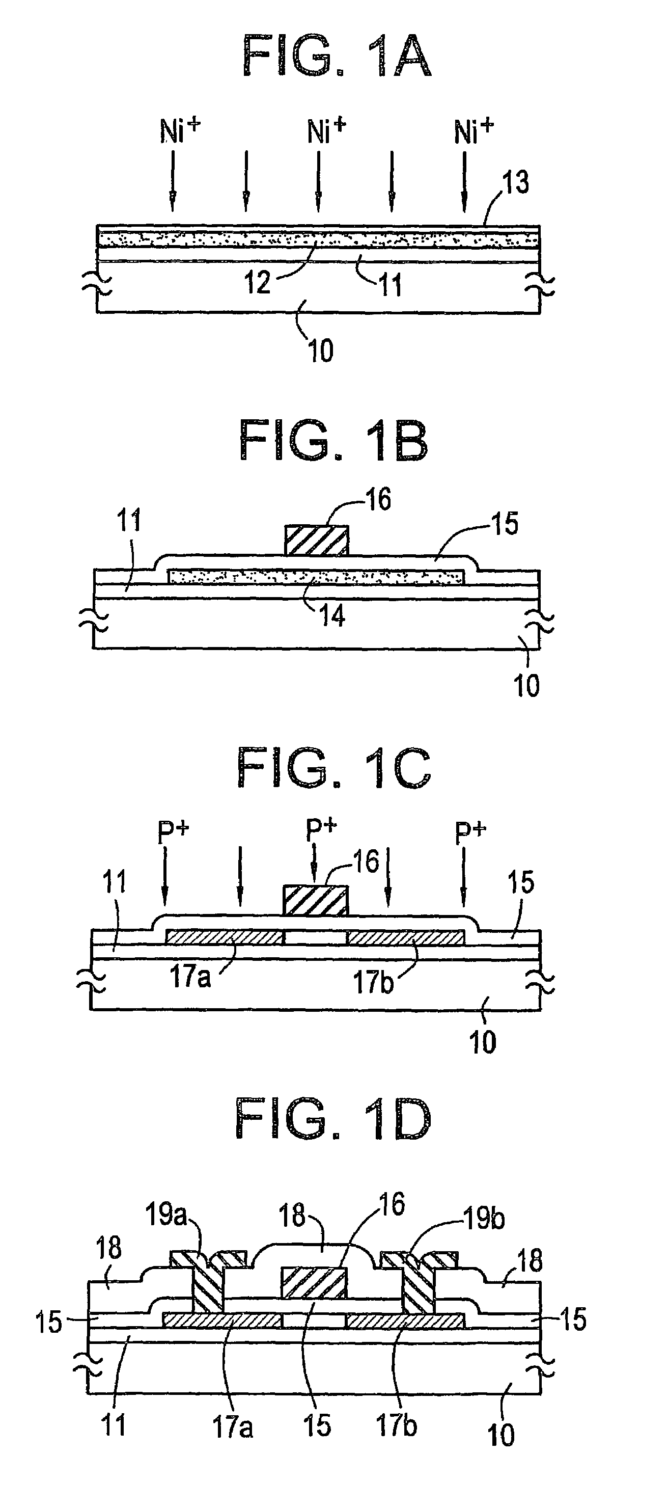
[0074]FIGS. 1A to 1D show cross sections of TFTs (Thin Film Transistors) illustrating the forming processes of the first embodiment. First, a base film 11 of silicon oxide having a thickness of 2000 Å is formed on a substrate 10 (Corning 7059) by sputtering. Then, an amorphous silicon film 12 of the intrinsic (I type) having a thickness of 500 to 1500 Å, e.g., 1500 Å, is formed on the base film 11 by plasma CVD (Chemical Vapor Deposition). Further, a silicon oxide film 13 having a thickness of 200 Å is formed on the amorphous silicon film 12 by sputtering. Subsequently, nickel ions are introduced into the amorphous silicon film 12 by ion implantation. The dose is 2×10¹³ to 2×1014 cm−2, e.g., 5×1013 cm−2. As a result, the concentration of the nickel in the amorphous silicon film 12 is about 5×1018 cm−3 (FIG. 1A).
[0075]The amorphous silicon film 12 is annealed at 550° C. for 4 hours in a nitrogen ambience to crystallize it. Thereafter, the amorphous silicon film 12 is pa...
embodiment 2
[Embodiment 2]
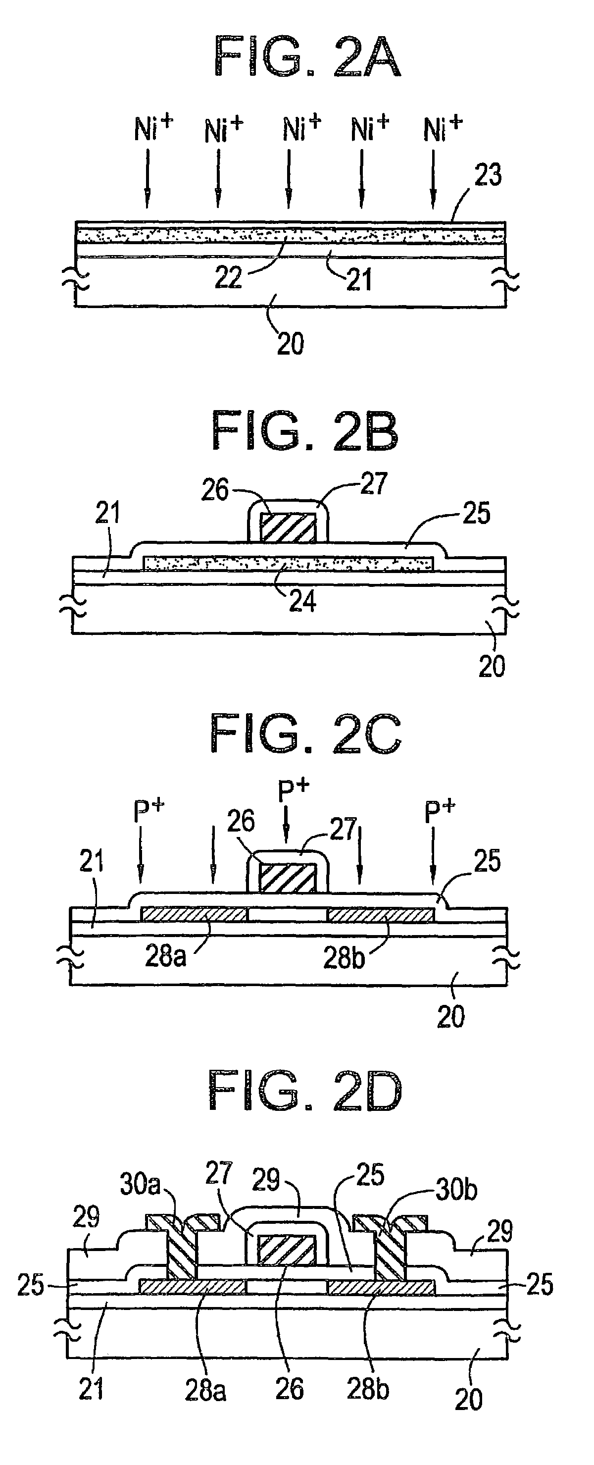
[0081]FIGS. 2A to 2D shows cross sections illustrating the forming processes of the second embodiment. First, a base film 21 of silicon oxide having a thickness of 2000 Å is formed on a substrate 20 (Corning 7059) by sputtering. An amorphous silicon film 22 of the intrinsic (I type) having a thickness of 500 to 1500 Å, e.g., 500 Å, is formed by plasma CVD. A silicon oxide film 23 having a thickness of 200 Å is deposited by sputtering. Nickel ions are introduced into the silicon film by ion implantation. The dose is 2×10¹³ to 2×1014 cm−2, e.g., 1×1014 cm−2. As a result, the concentration of nickel in the amorphous silicon film 12 is approximately 1×1019 cm−3 (FIG. 2A).
[0082]As the gate insulating film of crystalline silicon TFTs, a silicon oxide film 25 having a thickness of 1000 Å is formed from tetraethoxy silane (TEOS; Si(OC2H5)4) and oxygen as a raw material gases by plasma CVD. Trichloroethylene (C2HCl3) is used in addition to the raw material gases. Before the for...
embodiment 3
[Embodiment 3]
[0090]In Embodiment 3, a catalytic element for promoting crystallization is contained in an aqueous solution and applied to an amorphous silicon film. Then, the amorphous film is crystallized by heating. The crystallinity of the film is further enhanced by an anneal conducted at a higher temperature.
[0091]The process is described by referring to FIGS. 3A to 3D up to the point where a catalytic element, in the embodiment, nickel, is introduced. A substrate 41 made of quartz glass is used. This substrate has 100 mm×100 mm in size.
[0092]First, an amorphous silicon film having a thickness of 100 to 1500 Å is formed by plasma CVD or LPCVD. In this embodiment, the amorphous silicon film 42 having a thickness of 1000 Å is formed by plasma CVD (FIG. 3A).
[0093]To remove contaminants and the natural oxide film, the laminate is treated with hydrofluoric acid. Then, an oxide film 43 having a thickness of 10 to 50 Å is formed. If contamination can be neglected, the natural oxide fi...
PUM
 Abstract
Description
Claims
Application Information