[0009]The present invention enables a new regime of robust, ultra-high-precision
laser machining (UHPLM) where features are reduced by more than an
order of magnitude. Here is presented a versatile technique for
machining of nanometer-scale features using tightly-focused
ultrashort laser pulses. By the invention, the size of features can be reduced far below the
wavelength of light, thus enabling nanomachining of a wide range of materials. The features may be extremely small (<20 nm), are highly reproducible and are independent of the polarization of the light. This generalized process for nanoscale machining holds great promise for applications including MEMS construction and design,
microelectronics, fabricating optical wave-guides and memory,
microfluidics,
materials science,
microsurgery, and creating structures to interface with cells and biological molecules. The present invention will also anticipate significant
impact in the
biological sciences, enabling
targeted disruption of nanoscale cellular structures and genetic material.
[0011]This reduction arises not by further decreases in pulse widths, but by decreasing the
focal spot size using
high numerical aperture objectives, and carefully controlled approach to the optical damage energy threshold. The reduction of the photodisrupted
zone size from the initial
nanosecond studies to work by the present invention is at least three orders of magnitude, and here is shown to be over five orders of magnitude.
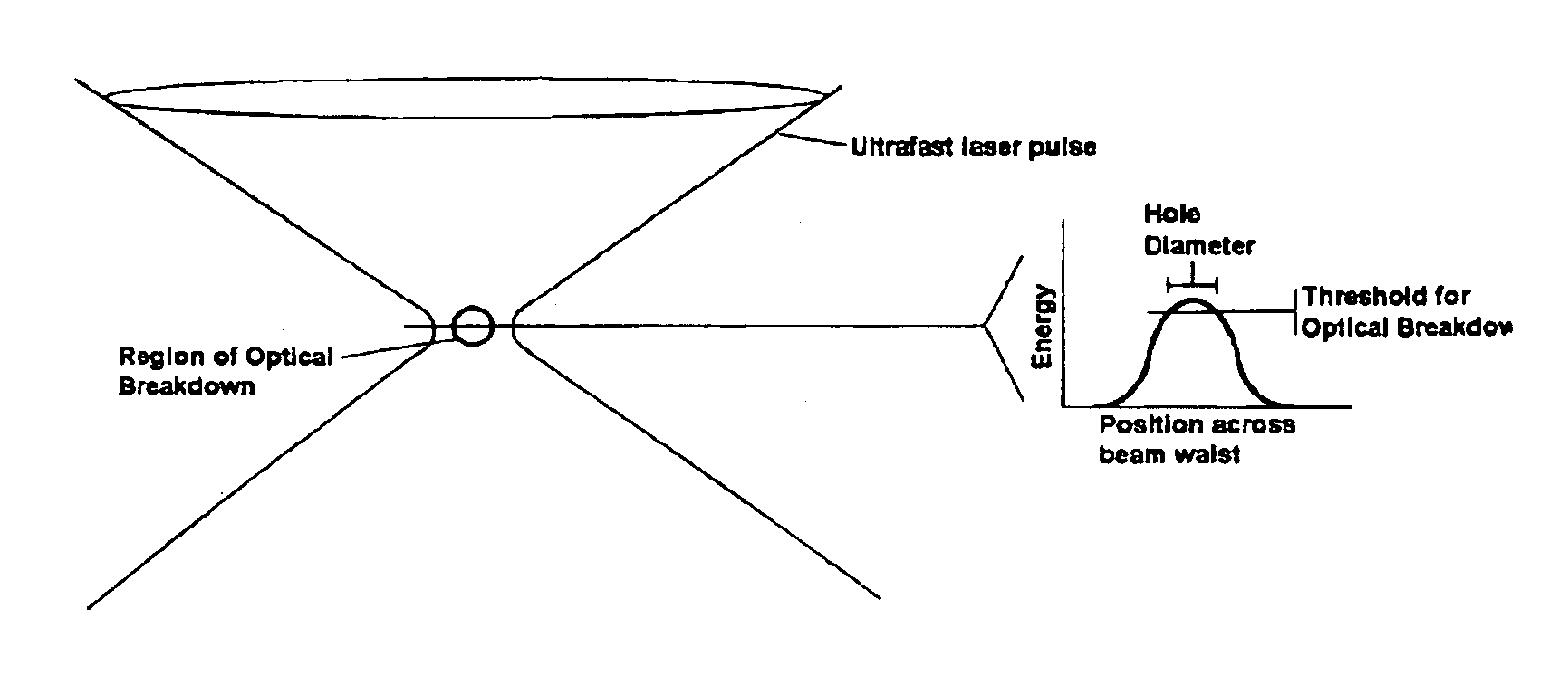
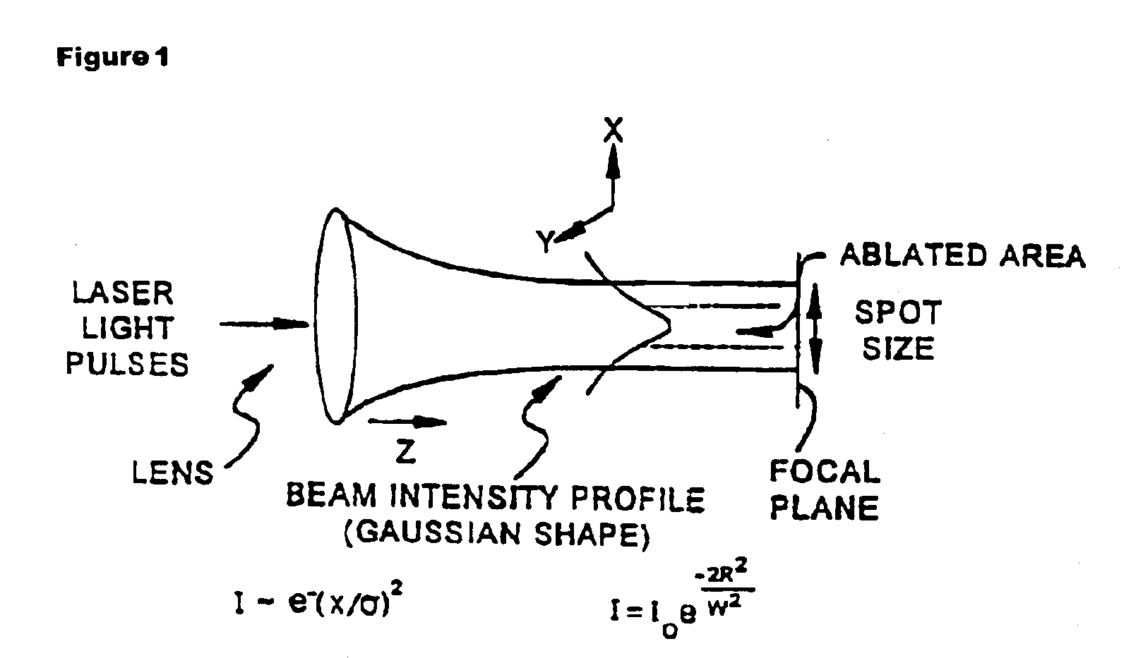
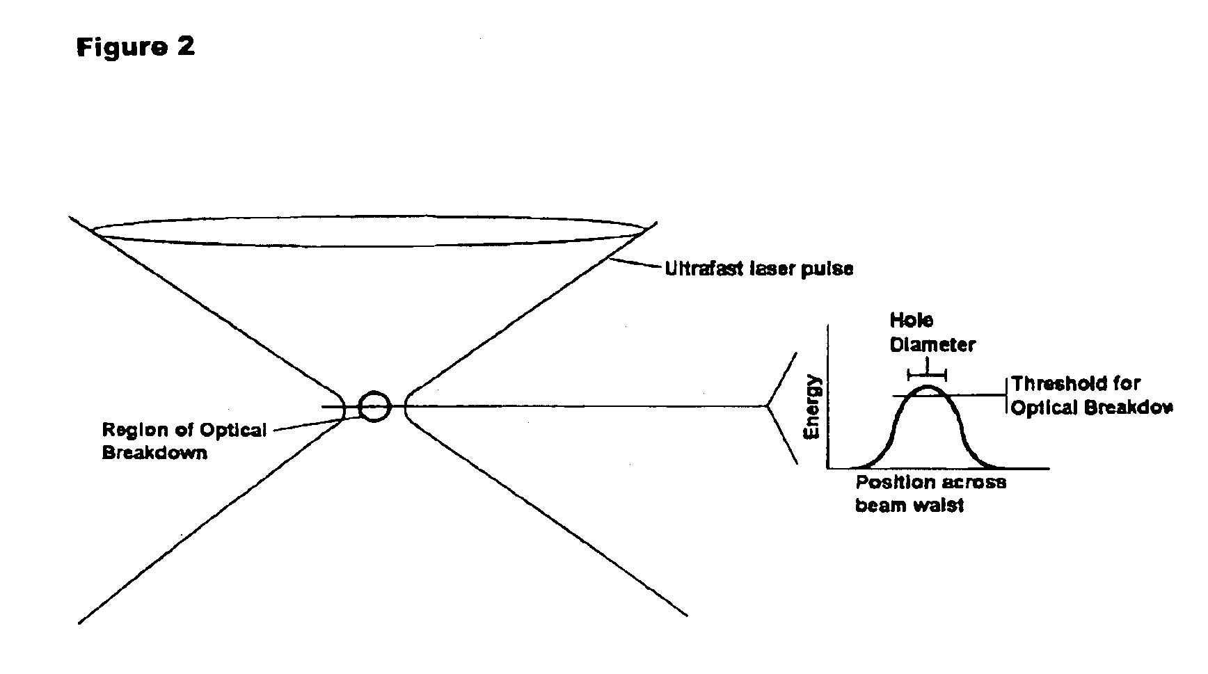
[0021]In one aspect, the method of the invention provides a
laser beam which defines a spot that has a lateral
gaussian profile characterized in that
fluence at or near the center of the beam spot is greater than the damage
threshold energy density whereby the
laser induced breakdown is
ablation of an area within the spot. The
maximum intensity is at the very center of the beam
waist. The beam
waist is the point in the beam where wave-front becomes a perfect plane; that is, its
radius of curvature is infinite. This center is at
radius R=0 in the x-y axis and along the Z axis, Z=0. This makes it possible to damage material in a very small volume centered on Z=0, R=0. Thus it is possible to make features smaller than spot size in the x-y focal plane and smaller than the Rayleigh range (
depth of focus) in the Z axis. It is preferred that the pulse width duration be in the
femtosecond range although
pulse duration of higher value may be used so long as the value is less than the pulse width defined by an abrupt or discernable change in slope of
fluence breakdown threshold versus laser
beam pulse width.
[0024]As can be seen, the present invention takes a new approach as compared to the prior work of U.S. Pat. No. 5,656,186, Mourou et al., which showed that when matter is subjected to focused high-power laser pulses localized plasmas are generated by
optical breakdown. As shown in this present invention, optical breakdown proceeds by Zener
ionization followed by a combination of Zener and Zener-seeded avalanche
ionization, in which initial (seed) unbound electrons in the target material are accelerated by the extreme
electric field of a
short pulse laser to create a
cascade of free electrons through collisions. This even occurs in transparent materials, which become opaque light absorbers above a certain
irradiance threshold.
Optical breakdown shows a highly non-linear dependence on intensity. This non-
linearity makes it possible to limit optical breakdown to regions smaller than the spot-size of the focused laser; the laser power can be selected so that only a small section of a
gaussian diffraction-limited focus exceeds the required intensity. This “
thresholding” effect is especially effective when exploiting the nearly deterministic nature of optical breakdown observed for sub-
picosecond pulses thus allowing fabrication of sub micron features. Here such benefits are further extended by new concepts for focusing,
pulse duration,
fluence, and intensity, and the invariance of damage
threshold energy density even at the nanometer scale. This is not predicted by previous work or theory, and precipitates a theoretical framework that indicates that contrary to common belief multiphoton
ionization is not involved, and ultra-high-precision is made possible by a mechanism dominated by Zener-seeded
impact ionization.

