Artificial synapse chip interface for electronic prosthetic retina

a technology of electronic prosthetic retina and synaptic synapse, which is applied in the direction of prosthesis, artificial respiration, therapy, etc., can solve the problems of permanent damage to photoreceptors, no effective treatment for most patients, visual impairment or blindness, etc., and achieves less power for stimulation, influence the behavior of a cellular system, and high spatial resolution

Inactive Publication Date: 2006-02-21
THE BOARD OF TRUSTEES OF THE LELAND STANFORD JUNIOR UNIV
View PDF6 Cites 55 Cited by
  • Summary
  • Abstract
  • Description
  • Claims
  • Application Information

AI Technical Summary

Benefits of technology

[0014]A reservoir may be directly in contact with a nanoaperture, or may be connected to a nanoaperture by a conduit effective to deliver neuromodulatory agents from the reservoir to the nanoaperture. Pumps or other fluid-directing mechanism may be operably connected to a reservoir and / or conduit effective to induce fluid flow which may, for example, be effective to aid the delivery of neuromodulatory agents to the nanoaperture.
[0017]The ability to direct neurite extension to form directed contacts with a circuit is useful in therapies for any disease of neural tissue. Thus, in one aspect of the invention, the devices and methods provide a neural interface that can bypass retinal photoreceptors and connect a digital camera to individual nerve cells in the retina. In this way, cells damaged in AMD and other blinding diseases can be bypassed and visual information sent to the brain. Thus, the artificial synapse chip provides methods for the restoration of visual function in patients suffering from blindness due to age-related macular degeneration (AMD), retinitis pigmentosa, and other photoreceptor blinding diseases. The devices and methods of the invention provide a neural prosthesis suitable for implantation in any location within the nervous system or body of a patient, for the treatment of spinal cord injuries, neuropathies, bladder dysfunction, and other diseases due to neuronal disorders.
[0020]Devices of the invention, each termed an “artificial synapse chip” (ASC), comprise a high-resolution neural interface to the visual system that incorporates micropatterned neuronal growth to produce an artificial synapse. The nanoapertures of a very small size, guided contacts with desired portions of individual cells, and targeted stimulation of individual cells via these contacts provide a neural interface with high spatial resolution for connecting a circuit to individual neurons. Thus, unlike previous methods for stimulating retinal neurons that offer only poor spatial resolution, the ASC provides the advantages of specificity and control of stimulation at a cellular level to provide novel ways to influence the behavior of a cellular system. In addition, since the source is in direct contact with the neuron, the ASC uses less power for stimulation than prior art field stimulators. The ASC thus provides a new class of regeneration electrodes—one that uses a novel neural interface for stimulation and that uses modern surface science methods for directing neuronal growth so that connection to in vivo neural circuitry in a retina is possible.

Problems solved by technology

Disturbances at any step in the process may lead to visual impairment or blindness.
Currently, there is no effective treatment for most patients with AMD, a disease that often results in permanent damage to photoreceptors, but spares most retinal ganglion cells (RGCs).
Similarly, other diseases such as retinitis pigmentosa (RP) cause vision impairment and blindness due to loss of photoreceptors.
Although these trials have demonstrated that vision is recoverable in a limited fashion, major challenges remain.
Due to the size and difficulties in placement of most available electrodes, imprecise electric field stimulation extending over long distances (several cell-body diameters) is used to depolarize neurons.
However, such methods often require excessive stimulation, which may be harmful, leading to inflammation of the stimulated region and even to excessive growth of glial cells, or gliosis.
Thus, an unmet major challenge of these approaches is that of constructing a neural interface that stimulates localized retinal regions, individual neurons, and even specialized portions of neurons with specificity.
However, the synaptic connections of neurons grown on artificial substrates may not be controlled or precisely directed to defined locations, and do not provide for the specific stimulation characteristics found in vivo.

Method used


Image

  • Artificial synapse chip interface for electronic prosthetic retina
  • Artificial synapse chip interface for electronic prosthetic retina
  • Artificial synapse chip interface for electronic prosthetic retina

Examples


example 1

Microfabrication of Apertures

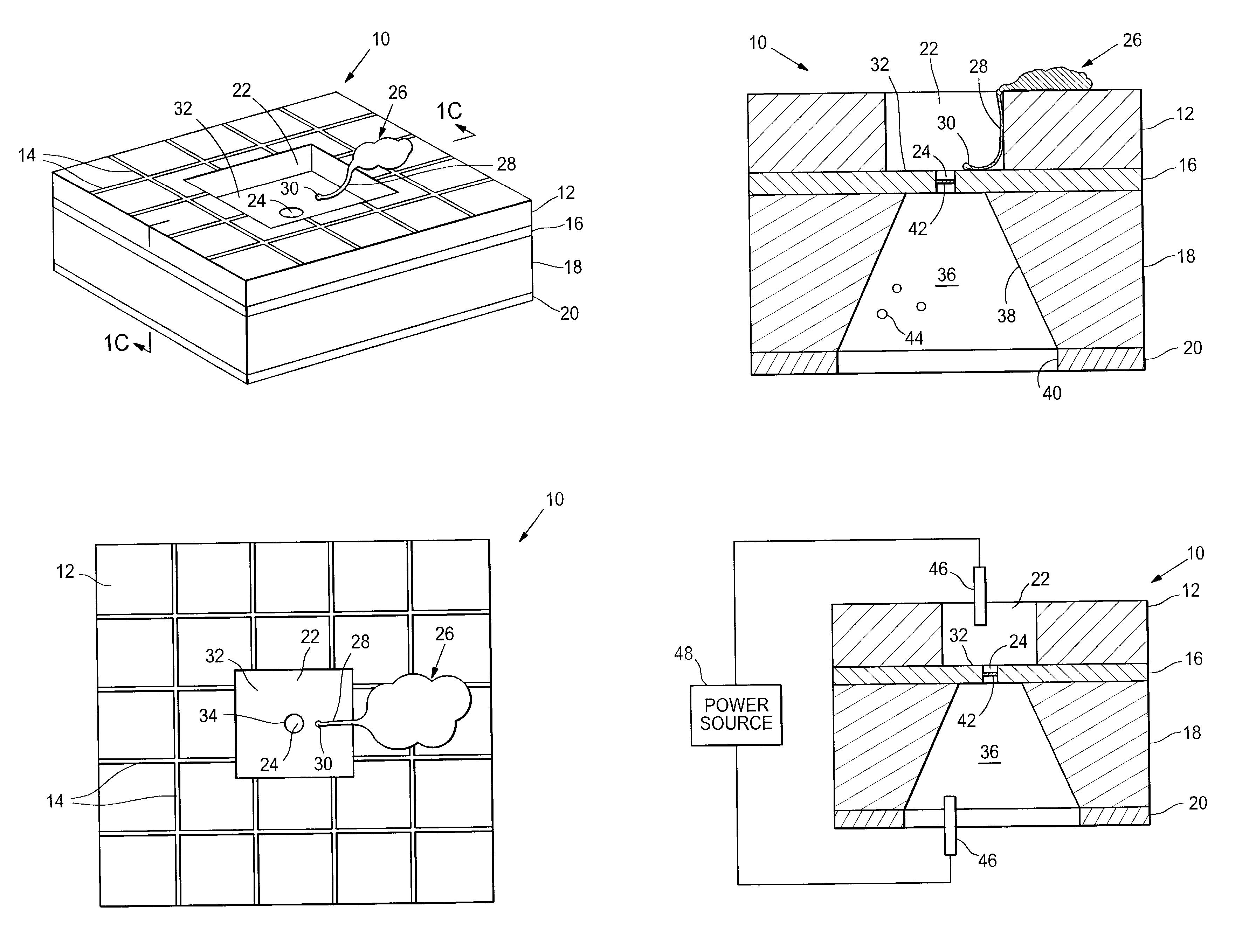
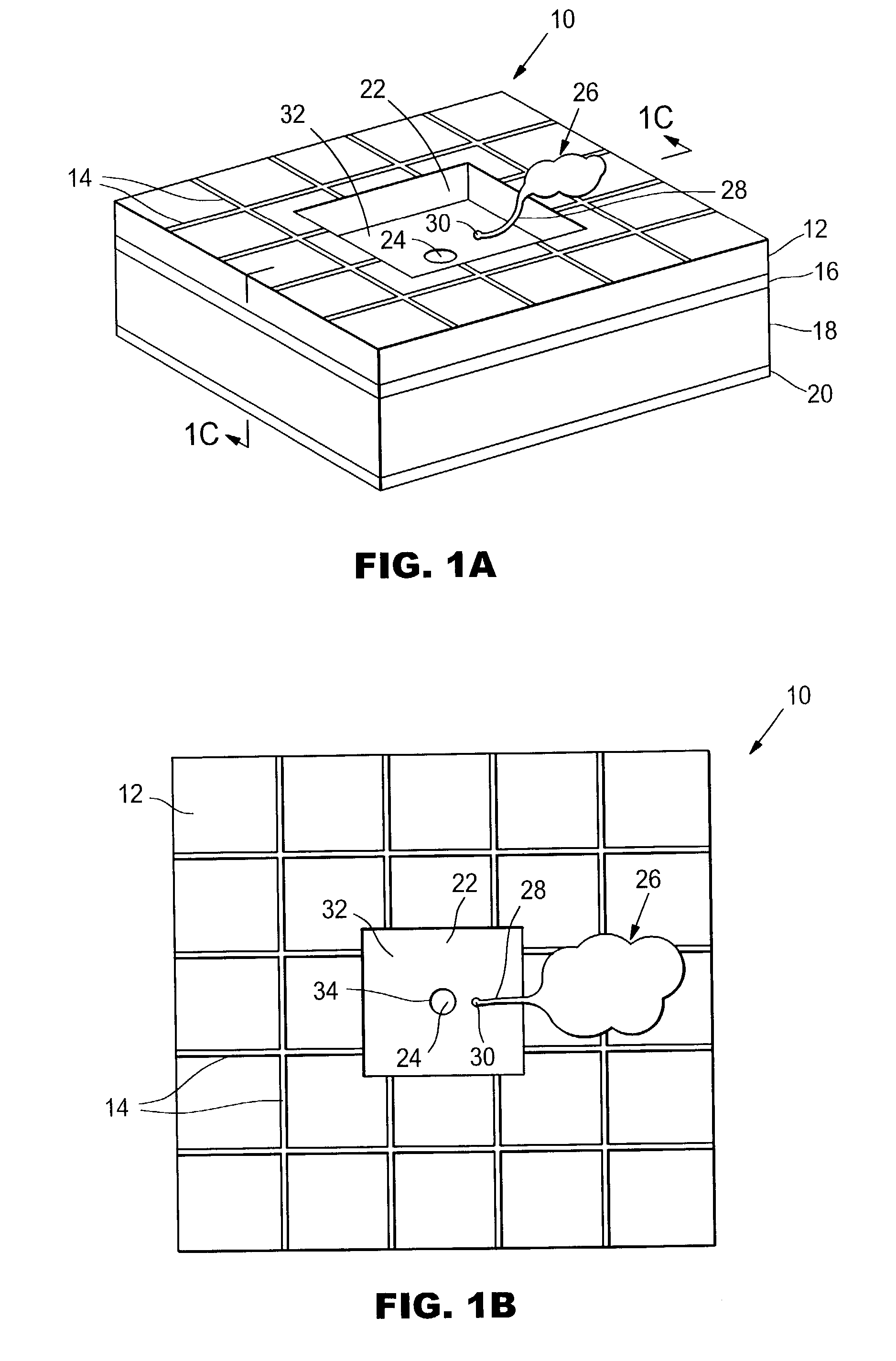
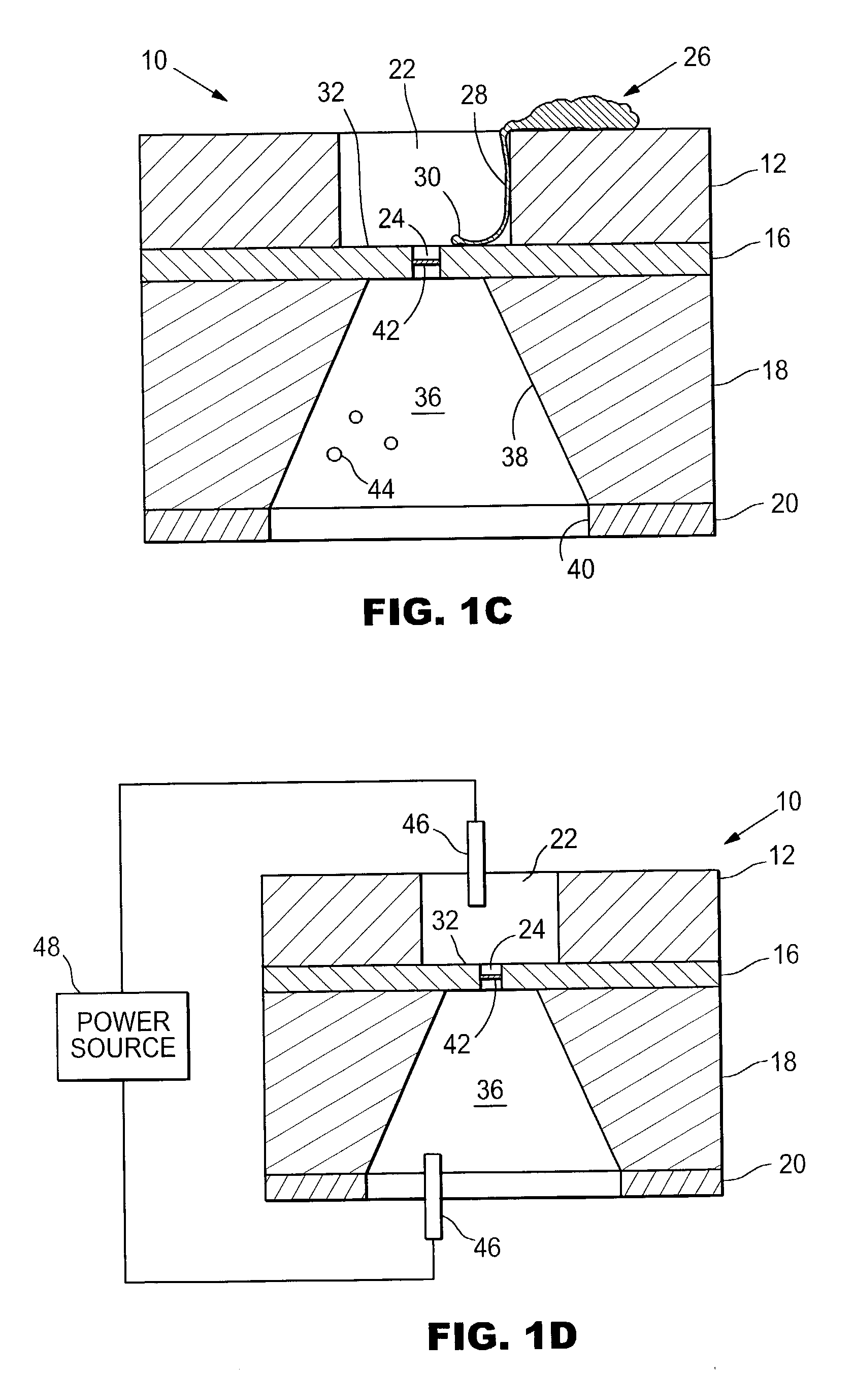
[0079]Microfabricated apertures on a silicon chip surfaces have been made using the Stanford Nanofabrication Facility. Microfabricated wells with microfabricated apertures are shown in FIG. 2. Standard silicon processing techniques were adapted for producing micrometer and nanometer-sized apertures in a silicon nitride membrane. Using low-pressure chemical vapor deposition (LPCVD), silicon nitride was grown on the surface of orientation silicon wafers. A combination of lithography to define the structures in a photosensitive polymer was followed by plasma etching to pattern the structures in the silicon nitride creates apertures on one side of the wafer and an etchant masking layer on the other side. An anisotropic etchant, such as tetramethylammonium hydroxide (TMAH), was used to remove the silicon along the {111} crystal plane, but leave the silicon nitride unaffected. This produced a via hole (a connecting passageway) beneath the aperture, exposing t...

example 2

Device Fabrication and Optimization

[0083]This Example describes the manufacture and optimization of devices embodying features of the invention for use in forming bilayer membranes across the microfabricated apertures of the devices. Chips were made with surface areas of about 1 cm2 and with a final thickness of roughly 0.5 mm. Circular apertures of 25 μm through 250 μm (diameter) were plasma etched in 500 nm thick silicon nitride. The chips were covered in a thick polyimide, except for a square region of exposed silicon nitride 500 μm on a side.

[0084]Fabrication was done at the Stanford Nanofabrication Facility (SNF) with 4 inch, orientation, boron-doped, double-polished silicon wafers, nominally 500 μm thick. Using low-pressure chemical vapor deposition (LPCVD), a thin layer (500 nm) of silicon nitride was grown on the surface of the wafers. Standard contact photolithography and plasma etching of the silicon nitride was used to define the small features (e.g., the apertures). The...

example 3

Bilayer Formation Across Silicon Nitride Apertures

[0093]Lipid bilayers were formed by the method of Montal and Mueller (1972). In practicing the Langmuir-Blodgett technique, one raises two lipid monolayers across an aperture, allowing the lipids to align their hydrophobic tail portions across the aperture so as to form a lipid bilayer. Because of the hydrophobic nature of the lipid tails, in order to form stable bilayers the surface of a BSP must also be hydrophobic. If the substrate is hydrophobic, the lipids can smoothly transition from coating the substrate to spanning the aperture. To reverse the wetting properties of the naturally hydrophilic silicon nitride, the silicon nitride was coated with an alkylsilane (octyltrichlorosilane). Application of this coating was quite simple and very effective. It was not found to be possible to form a bilayer with untreated devices. Use of longer carbon chain silanes or alternative materials to make the surface even more hydrophobic would fu...


PUM

PropertyMeasurementUnit
thickaaaaaaaaaa
diameteraaaaaaaaaa
diameteraaaaaaaaaa

Abstract

The invention provides microfabricated devices and methods for directing the growth of a cell process to form an artificial synapse. The devices are called artificial synapse chips. The artificial synapse comprises a nanofabricated aperture (about 50–100 nm in size) that connects the cell process to a chemical or electrical means of neuronal excitation. Such an aperture width mimics the length scales of a natural synapse and thus emphasizes the localized spatial relationship between a neuron and a stimulation source. The invention further provides devices and methods for regenerating a nerve fiber into an electrode. The invention thus provides a regeneration electrode that uses a novel neural interface for stimulation and that uses novel surface methods for directing neuronal growth making possible in vivo connection of the devices to neural circuitry in a retina and other anatomical locations.

Description

CROSS REFERENCE TO RELATED APPLICATION[0001]This application is related to and claims priority under 35 U.S.C. § 119(e) from U.S. Provisional Application Serial No. 60 / 301,934, entitled “ARTIFICIAL SYNAPSE CHIP INTERFACE FOR ELECTRONIC PROSTHETIC RETINA”, by Fishman et al., filed Jun. 29, 2001, which is hereby incorporated by reference in its entirety.FIELD OF THE INVENTION[0002]The invention pertains to the devices for controlling cell growth and for stimulating cells. In particular, the invention is directed to methods and devices for controlling neuronal growth to provide artificial synapses and neural prostheses.BACKGROUND OF THE INVENTION[0003]Light entering the eye through the cornea is focussed through the lens (which further focuses the light) onto the retina, a thin layer of cells in the back of the eye. Normal human vision depends upon signals generated by nerve cells in the retina. The visual signals originate with the photoreceptor cells in the retina, which sense and re...

Claims


Application Information

Patent Timeline
Patent Type & Authority Patents(United States)
IPC IPC(8): A61F2/14A61K9/22A61L27/00A61N1/05A61N1/36C12M1/42C12M3/00C12N5/0793
CPCC12M35/02C12M35/08C12N5/0619C12M35/00A61N1/0543A61N1/326A61N1/36046C12N2503/00C12N2535/10
Inventor FISHMAN, HARVEY A.BLUMENKRANZ, MARKBENT, STACEY F.BLOOM, DAVID M.PETERMAN, MARK C.
Owner THE BOARD OF TRUSTEES OF THE LELAND STANFORD JUNIOR UNIV
Why Eureka
Try Eureka