Manufacturing method of semiconductor device

a manufacturing method and semiconductor technology, applied in the field of semiconductor devices, can solve the problems of lack of thermal stability, easy damage by charged particles, and silicon oxide isolating films, etc., and achieve the effects of high reliability, good quality and fineness, and high performan

Inactive Publication Date: 2006-08-29
SEMICON ENERGY LAB CO LTD
View PDF33 Cites 25 Cited by
  • Summary
  • Abstract
  • Description
  • Claims
  • Application Information

AI Technical Summary

Benefits of technology

[0010]The present invention has been made in view of the above problems and an object of the present invention is to provide a technique for forming the insulating film of good quality and fineness that is applicable to a transistor made on a substrate weak against heat such as a glass and a semiconductor device that can realize high performance and high reliability using the technique. Also, another object of the present invention is to provide the semiconductor device having a large area integrated circuit that a transistor made of superior insulating layers is used as a component element.
[0014]A representative form of a manufacturing method of a semiconductor device according to the present invention is to form a silicon oxide film and a silicon nitride film on a crystalline semiconductor film by a high-frequency sputtering method, subject the films to heat treatment, and then, form a conductive film thereon with a DC sputtering method with metal as a target. Since all the steps that are described above are continuously performed without exposing the films to the atmosphere, physical contamination due to particulates or the like and chemical contamination due to an environment around the films are prevented and a clean interface can be formed.
[0016]In the sputtering method applied in the present invention, only oxygen gas or nitrogen gas can be used as a sputtering gas. During high-frequency discharge of oxygen or nitrogen, various ion species, excited species, and luminous species, and various radicals (chemically active species which is electrically neutral and high in responsiveness) are formed. The inventors found that, among them, an oxygen radical or a nitrogen radical having a chemically extremely active characteristic is generated, and the oxygen radical or the nitrogen radical can react with silicon serving as a target material to form a dense film. That is, the oxygen radical or the nitrogen radical diffused on the surface of the target reacts with silicon to form an oxide or a nitride. Although the oxide or the nitride formed on the surface of the target is stable, when an ion is accelerated in a sheath electric field and incident on the surface, the oxide or the nitride is sputtered to be emitted into a gas phase and deposits on a substrate (including a reaction process in the gas phase), thereby making it possible to form a film.
[0020]Moreover, the heat treatment performed at the temperature of 600 to 800° C. acts effectively in order to reduce silicon clusters contained in the silicon oxide film or the silicon nitride film and remove distortion of an interface. This action of the heat treatment has been confirmed in capacitance characteristics of a MOS structure, and it has been proved that hysteresis is reduced by the heat treatment in the above-mentioned temperature range. A characteristic of the stacked body of the silicon oxide film and the silicon nitride film of the present invention is that, in a C-V characteristic of the MOS structure, a fluctuation value of a flat-band voltage due to hysteresis before and after a bias thermal stress test (BT test) is 0.5 V or less, preferably 0.3 V or less. This fluctuation value of the flat-band voltage is a numerical value which is attained by the heat processing at 600 to 800° C. By specifying the fluctuation value of the flat-band voltage in the C-V characteristic of the MOS structure, a stacked body of a silicon oxide film and a silicon nitride film with a low fixed charge density or interface level density is selected, and a stable current voltage characteristic without hysteresis can be obtained in a transistor.
[0023]Application of the stacked body of the silicon oxide film and the silicon nitride film to a gate insulating film means substantial thinning of the gate insulating film. Since a relative dielectric constant of the silicon nitride is approximately 7.5 as opposed to 3.8 of the silicon oxide, by containing the silicon nitride film in a gate insulating film formed of the silicon oxide film, an effect substantially equivalent to realizing thinning of the gate insulating film can be obtained, and it becomes possible to reduce gate leak. An advantageous effect can be obtained with respect to refining of elements based upon a scaling rule. Moreover, by using a dense silicon nitride film as a constituent member of the gate insulating film, the gate insulating film can be caused to function as a protective film for preventing intrusion of impurities from the outside, and a clean interface can be formed between the gate insulating film and the semiconductor film.

Problems solved by technology

However, insulating films such as silicon oxide and silicon nitride that are deposited using chemical or physical reaction by conventional plasma CVD or sputtering method have a disadvantage such as defect and pinholes resulted from being easily damaged by charged particles, fixed charge or high interface state level.
Also, it lacks in a thermal stability due to several atoms percent of hydrogen contained in the insulating film.
And it is also a cause of a characteristic deterioration such as fluctuation in a threshold voltage or increase of a gate leak current.

Method used


Image

  • Manufacturing method of semiconductor device
  • Manufacturing method of semiconductor device
  • Manufacturing method of semiconductor device

Examples


embodiment mode 1

[Embodiment Mode 1]

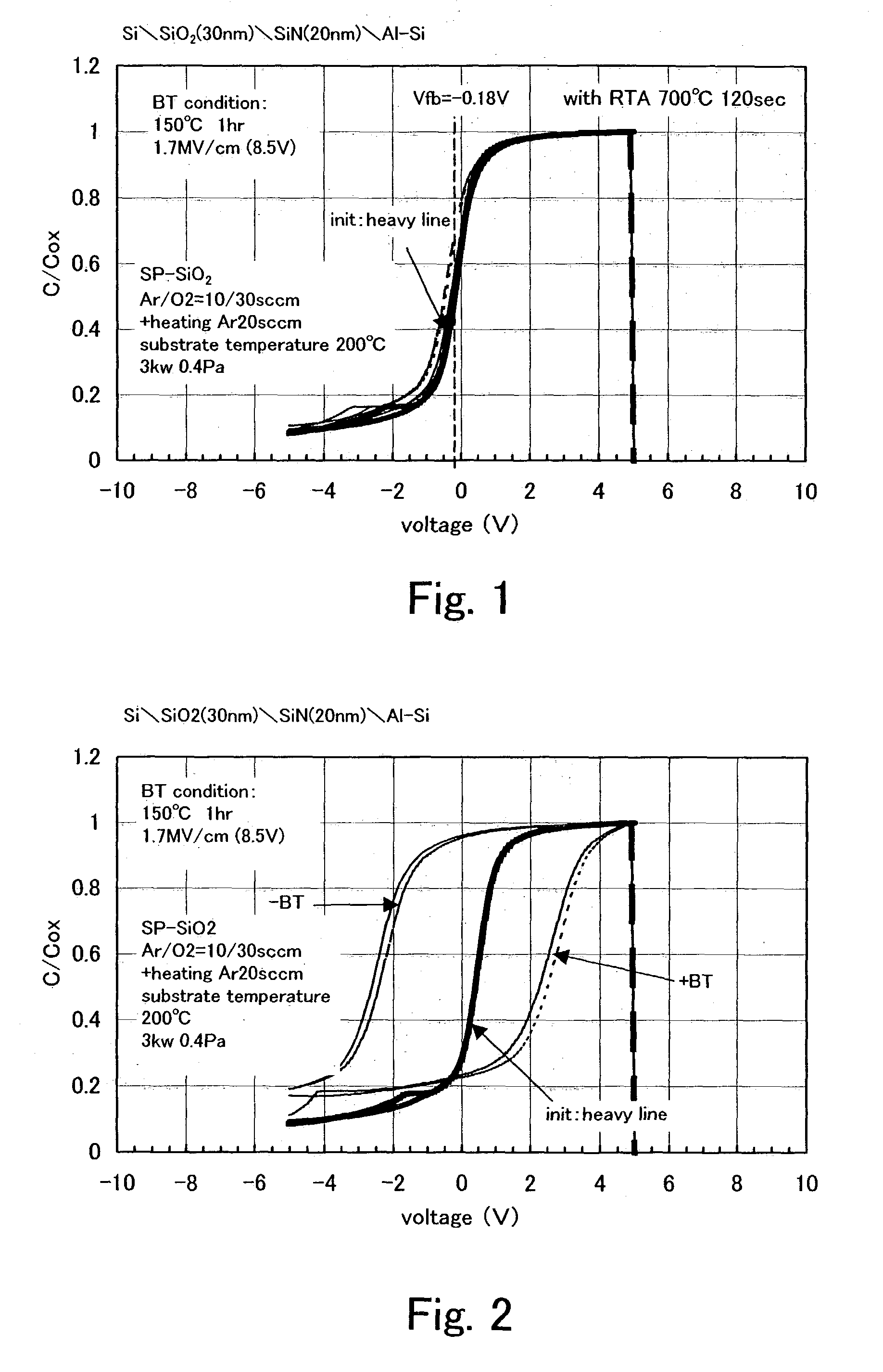
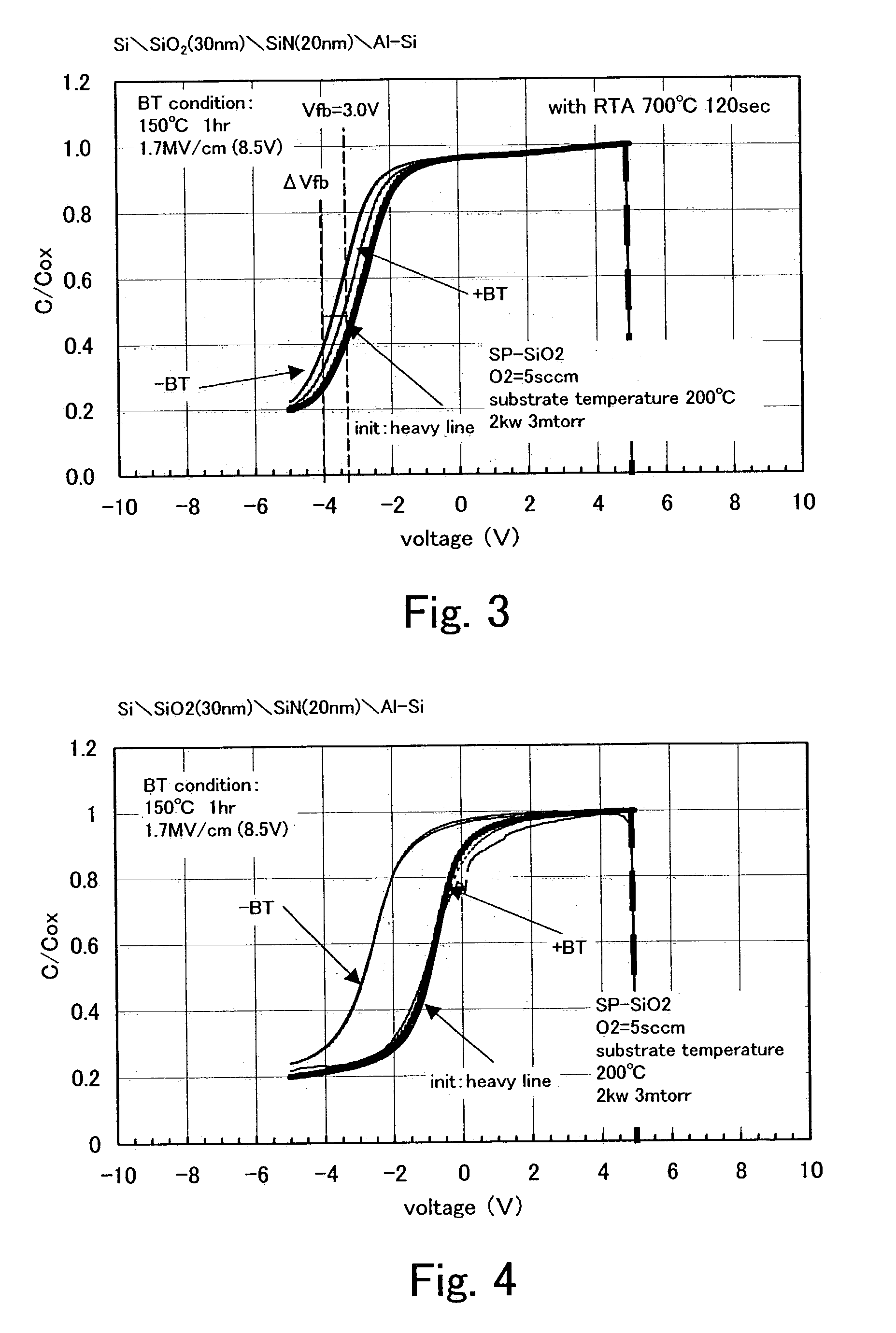
[0045]A stacked body of a silicon oxide film, which is formed by the sputtering method by applying high-frequency power in an atmosphere containing oxygen or oxygen and a rare gas using silicon as a target, and a silicon nitride film, which is formed by the sputtering method by applying high-frequency power in an atmosphere containing nitrogen or nitrogen and a rare gas is used as a gate insulating film of an insulated gate field effect transistor, which is a main component of a semiconductor device, typically a thin film transistor (TFT). The stacked body is deposited and formed at a substrate heating temperature of 400° C. or less, preferably 300° C. or less and is thereafter capable of reducing a defect density on a stacked layer interface or a defect density in a film and distortion by a heat treatment at a temperature higher than that. Preferably by performing a heat treatment at the temperature of 600 to 800 ° C., and particularly preferably by performing ra...

embodiment mode 2

[Embodiment Mode 2]

[0070]An embodiment mode of forming a semiconductor device on a glass substrate with a distortion point of 700° C. or less will be described in relation to a structure in which a stacked body, which is obtained by stacking a silicon oxide film and a silicon nitride film manufactured by the high-frequency sputtering method using silicon as a target and subjected to a heat treatment, is incorporated as a gate insulating film for a TFT.

[0071]As a substrate which can be applied in this embodiment mode, a glass substrate containing barium borosilicate glass, alumino borosilicate glass, alumino silicate glass, or the like as a material is suitable. Representatively, a 1737 glass substrate (distortion point 667° C.) manufactured by Corning Incorporated, AN 100 (distortion point 670° C.) manufactured by Asahi Glass Co., Ltd., and the like are applicable. However, it goes without saying that other similar substrates may be applied without any specific limitation. In any ca...

embodiment mode 3

[Embodiment Mode 3]

[0094]After the crystalline silicon film shown in FIG. 9B is obtained in Embodiment Mode 2, a laser oscillator using crystals of YAG, YVO4, YLF, YalO3, or the like doped with Cr, Nd, Er, Ho, Ce, Co, Ti, or Tm is applied to the film as a solid state laser of a continuous oscillation type as shown in FIG. 12. A basic wave in the laser oscillator is different depending upon a material to be doped, and a laser beam having the basic wave of about 1 μm is obtained. A higher harmonic wave as opposed to the basic wave can be obtained by using a nonlinear optical element. In the case in which the above-mentioned laser oscillator is used, a wavelength in a visible light region is substantially obtained with a second harmonic and a wavelength of an ultraviolet region is substantially obtained with a third harmonic. Representatively, an Nd:YVO4 laser oscillator (basic wave: 1064 nm) is used to apply a second harmonic thereof (532 nm). Laser beams of this oscillator are conden...


PUM

PropertyMeasurementUnit
temperatureaaaaaaaaaa
power frequencyaaaaaaaaaa

Abstract

It is an object of the present invention is to provide a technique for forming a dense insulating film of good quality that is applicable to a transistor made on a substrate weak against heat such as a glass and a semiconductor device that can realize high performance and high reliability using the technique. In the present invention a silicon oxide film is formed on a crystalline semiconductor film, which is formed on an insulating surface, by the sputtering method using silicon as a target by applying high-frequency power in an atmosphere containing oxygen or oxygen and a rare gas, a silicon nitride film is formed thereon by applying high-frequency power in an atmosphere containing nitrogen or nitrogen and a rare gas, and then, heat treatment of a stacked body of the crystalline semiconductor film, the silicon oxide film, and the silicon nitride film at a temperature higher than a temperature for forming the films is performed.

Description

BACKGROUND OF THE INVENTION[0001]1. Field of the Invention[0002]The present invention relates to a semiconductor device including an insulating film made by high frequency sputtering method using silicon as a target and a manufacturing method of the same. More particularly, the present invention relates to a gate structure of an insulated gate field effect transistor, typified by a thin film transistor (TFT).[0003]2. Description of the Related Art[0004]It is a known technique is that a TFT formed on a substrate such as a glass substrate, a liquid crystal or an electroluminescence (EL) material and a pixel combined with an element thereof is arranged in a matrix to make a display showing characters or images. A TFT, wherein a channel portion overlapped with a gate electrode is formed with a polycrystalline silicon film, can operate a logic circuit or the like at a suitable frequency.[0005]A polycrystalline silicon film for this purpose is an amorphous silicon film crystallized by a l...

Claims


Application Information

Patent Timeline
Patent Type & Authority Patents(United States)
IPC IPC(8): H01L21/84H01L21/20H01L21/00H01L21/314H01L21/316H01L21/318H01L21/336H01L21/77H01L27/12H01L29/786
CPCH01L21/02164H01L21/0217H01L21/022H01L21/02266H01L21/31612H01L21/3185H01L29/78675H01L21/67248H01L27/12H01L27/1214H01L29/66757H01L29/78621H01L21/67109H01L27/1255H01L27/1259
Inventor AKIMOTO, KENGOTAKAYAMA, TORUYAMAGUCHI, TETSUJIYAMAZAKI, SHUNPEI
Owner SEMICON ENERGY LAB CO LTD
Why Eureka
Try Eureka