Super lattice modification of overlying transistor

a transistor and super lattice technology, applied in the field of wide bandgap semiconductors, can solve the problems of affecting the surface roughness of the surface, and the inability to meet the lattice, so as to reduce the surface mobility of aluminum, reduce the roughness of the surface, and increase the performance of the resulting device

Active Publication Date: 2006-09-26
INFINEON TECH AMERICAS CORP
View PDF69 Cites 58 Cited by
  • Summary
  • Abstract
  • Description
  • Claims
  • Application Information

AI Technical Summary

Benefits of technology

[0010]The invention is a structure and a technique that allows a variety of unpatterned substrates to be used by employing a planarizing multi-layer structure. The structure is integrated into the growth of the epitaxial material and reduces the roughness of the surface while selectively deflecting or filtering threading dislocations. In one embodiment, this structure comprises a superlattice of alternating alloys of GaN and AlGaN. Alternatively, other alloys such as InGaN or AlInGaN may also be used.
[0011]The efficacy of the dislocation filter stems from the fact that GaN and AlGaN have slightly different lattice constants. The lattice constant of AlxGa1-xN is linearly dependent on the magnitude of x. There is built-in biaxial stress and strain when AlGaN is grown atop GaN. The resulting strain field serves as a barrier to propagation of dislocations with a component parallel to the normal growth direction. The addition of aluminum to the alloy during growth serves as a smoothing agent due to the reduced surface mobility of the aluminum (as compared to gallium adatoms).
[0012]While the amount of strain necessary to deflect the threading dislocations depends on the details of crystal growth—temperature, flow, precursors, substrate, composition, dislocation density, etc., this invention can create a 20 to 50% increase in the performance of the resulting devices.

Problems solved by technology

There are currently no cost effective, lattice matched substrates on which these crystalline materials can be grown.
As the crystal grows, the window tends to overgrow the masked area.
The disadvantage of this technique is that the substrate must be patterned and, in turn, area is sacrificed.

Method used


Image

  • Super lattice modification of overlying transistor
  • Super lattice modification of overlying transistor
  • Super lattice modification of overlying transistor

Examples


working examples

[0068]The invention will be further illustrated through the following examples.

working example 1

[0069]A device in accordance with the invention was fabricated as follows.

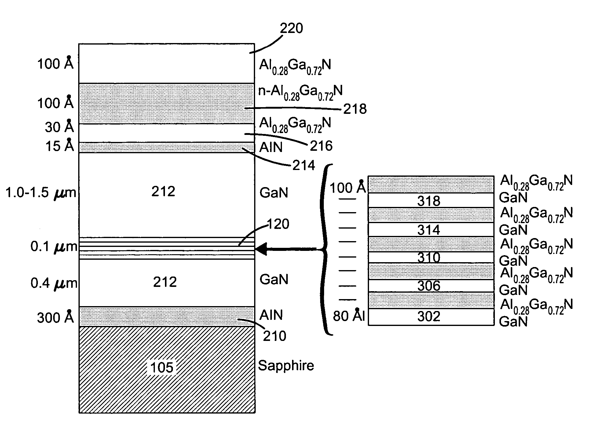
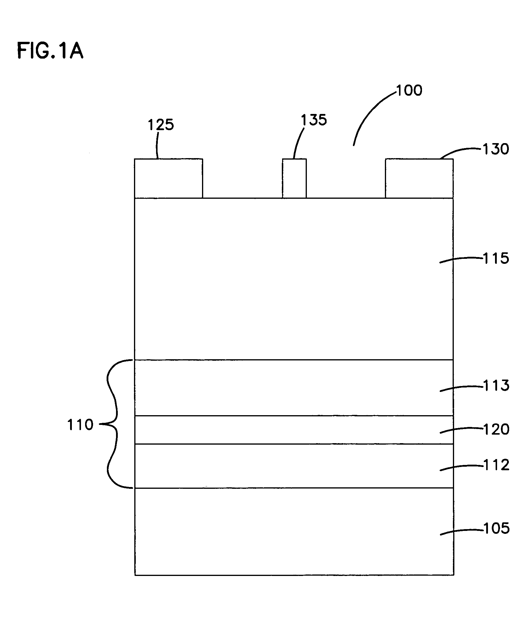
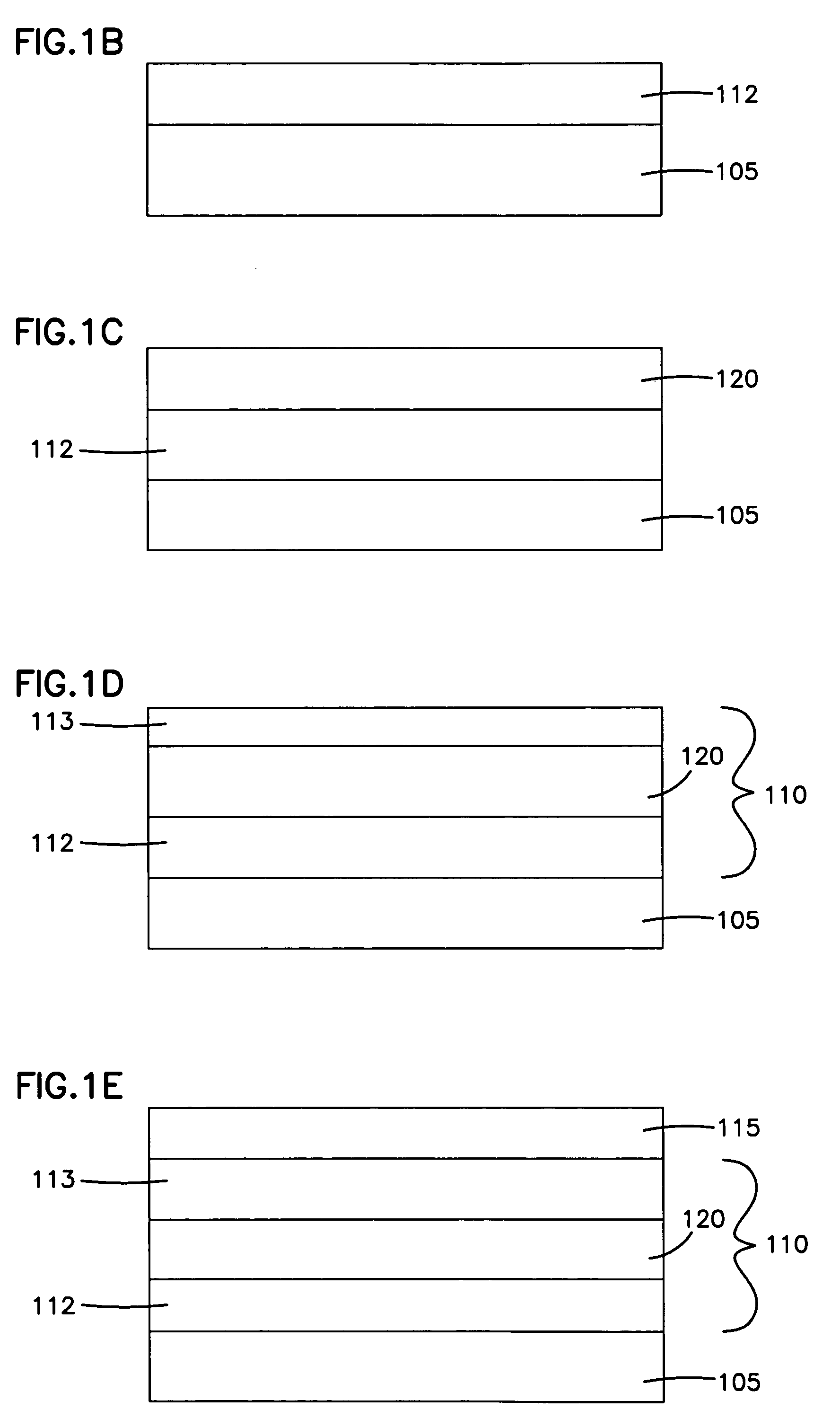
[0070]A degreased and etched (0001) basal plane sapphire substrate (1.25 inch diameter) was loaded on the SiC-coated graphite susceptor of a low-pressure metalorganic chemical vapor deposition (LP-MOCVD) vertical reactor with an inductive RF heater. All growth steps were carried out at 76 Torr using triethyl gallium at a flux of about 2 mg / min, triethyl aluminum at a flow of about 100 μg / min, ammonia at a flow of about 1.5 sl / min, and dilute disilane where necessary.

[0071]A conventional low-temperature (640° C.) buffer layer of AlN of about 300 Å was grown (growth time of about 5 minutes) was followed by high-temperature (˜1000° C.) undoped GaN (0.5 μm grown for about 20 minutes). Next, the superlattice of 5 periods (10 layers) of alternating layers of Al0.02Ga0.98N / GaN (0.1 μm) was deposited without any growth interruption at about 1000° C. Each GaN layer was about 80 Å thick (growth time about 1 minute 30 se...

working example 2

[0072]The device fabricated in Example 1 was then evaluated as follows.

[0073]Several techniques were employed to evaluate the structure including differential interference contrast (DIC) (Nomarski) microscopy, room temperature van der Pauw Hall measurements, high resolution x-ray diffraction (HRXRD), scanning electron microscopy (SEM) with selective etching, atomic force microscopy (AFM), and depletion capacitance-voltage depth profiling.

[0074]All growths showed mirror like flatness when examined using DIC microscopy (results not shown). The mobility and carrier concentration were measured by van der Pauw Hall technique immediately after growth.

[0075]Room temperature Hall effect measurements were made using van der Pauw technique. An increase of 2-DEG mobility from 1200 cm2 / V s (without superlattice) to 1500 cm2 / V s (with superlattice) was obtained with an increase in the carrier density from 1.1 to 1.4×1013 cm−2. The trend likely reflects changes in the planarity of the heterointer...


PUM


Abstract

The invention provides a device having a substrate, a buffer region positioned upon the substrate, wherein the buffer region has an upper buffer region and a lower buffer region, a heterojunction region positioned upon the buffer region, and a superlattice positioned between the lower buffer region and the upper buffer region, wherein the device is configured to function as a heterojunction field effect transistor.

Description

[0001]This application claims priority to U.S. Provisional Application No. 60 / 428,856 filed on Nov. 25, 2002 entitled SUPER LATTICE MODIFICATION OF OVERLYING TRANSISTOR, the disclosure of which is incorporated by reference herein.FIELD OF THE INVENTION[0002]The invention relates generally to wide bandgap semiconductors and their fabrication. More specifically, the invention relates to wide bandgap semiconductor devices comprising alloys including aluminum, gallium, nitrogen, and indium, and the fabrication of these devices.BACKGROUND OF THE INVENTION[0003]Gallium nitride and aluminum gallium nitride are wide bandgap semiconductors used in the production of such electrical and opto-electronic devices as blue light emitting diodes, lasers, ultraviolet photodetectors, and power transistors. There are currently no cost effective, lattice matched substrates on which these crystalline materials can be grown. Common exemplary substrates for the growth of these materials are sapphire, silic...

Claims


Application Information

Patent Timeline
Patent Type & Authority Patents(United States)
IPC IPC(8): H01L29/732H01L31/0328H01L21/335H01L29/15H01L29/20H01L29/778
CPCH01L29/155H01L29/7787H01L29/66462H01L29/2003
Inventor MUNNS, GORDON
Owner INFINEON TECH AMERICAS CORP
Why Eureka
Try Eureka