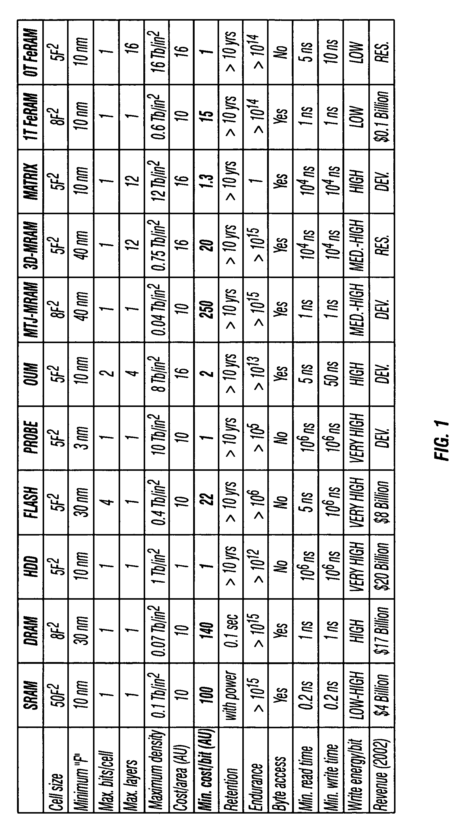
The scaling limits indicated for each solid-state technology are speculative and are based primarily on physical limits rather than current technical challenges.
Four technologies may eventually reach a cost that is comparable to that of HDDs through either multi-bit storage or 3-D integration, which are two characteristics that HDDs cannot practically possess.
Two of the four technologies, PROBE memories and MATRIX memories, are likely to have performance characteristics that are inferior to HDDs.
DRAM memory has very serious scaling challenges.
For example, one of the most serious scaling obstacles for
DRAM memory results from the adverse effects of
radiation in which a single
alpha particle can create about 1 million minority carriers that sometimes end up on the
capacitor.
In
DRAM, reading the state of the
capacitor is destructive, so the data must be rewritten afterward.
An
aspect ratio of this magnitude does not appear to be capable of being increased much further and soon capacitors will need to
flare out under the
silicon surface taking the shape of, for example, a
bottle.
Unfortunately, high-k dielectrics have a high leakage and, therefore, need a thickness that is thicker than that of the
dielectric materials that are used today.
With such scaling obstacles, it seems unlikely that DRAM will scale to be smaller than about 30 nm.
The areal density
advantage of HDDs, however, is likely to decrease due to the superparamagnetic limit in which scaling of magnetic grain size in the disk is no longer possible because
thermal energy kBT begins to compete with the
magnetic anisotropy energy KuV.
Nevertheless, there is a limit when
thermal energy kBT begins to compete with the Zeeman energy 2HAMsV, in which HA is the applied field, so that the grains are not properly oriented during writing.
Unfortunately, there is no known practical way to make a nanometer-scale heat spot on the disk.
The cost of FLASH memories, however, is rapidly dropping and is expected to be the fastest growing
memory type over the next few years, especially for NAND and AND-type
FLASH memory architectures.
Although multi-bit storage techniques reduce estimated cost dramatically, multi-bit storage typically leads to lower performance because the read / write process is more complicated.
FLASH memory, however, has very serious scaling challenges because the
dielectric around the floating gate must be at least 8 nm thick to retain charge for ten years.
NOR FLASH memory is not believed to be scalable past the 65 nm node due to problems with drain-induced barrier lowering during
programming at this
length scale.
Similarly,
NAND FLASH memory is projected to have very serious scaling challenges below 40 nm due to interference between adjacent gates, particularly for multi-bit storage.
Below this size, the small number of electrons per bit, the size of the
high voltage circuits, and interference between charge storage regions will likely cause obstacles too significant for further scaling.
Power dissipation, however, is very high for both reading and writing because micron-scale heaters are used at temperatures of up to 400 C dissipating about 5 mW each.
PROBE storage is inherently 2-D in nature and is not likely to be capable of multi-bit storage due to
noise and other issues, although in theory there could be three
layers of
polymer with different
glass transition temperatures to vary the depth with applied temperature and store 2 bits per indent.
So far, the estimated cost per unit area is uncertain, but is likely to be at least as expensive as other solid-state memories because two
silicon wafers are used in a precise sandwich arrangement and a substantial amount of
peripheral control circuitry is needed.
Alignment and thermal drift are a major problem and it is likely that a number of
thermal sensors and compensation heaters will be needed to keep top and bottom wafers isothermal and to within one degree of each other.
Tip wear and
polymer durability are other major issues.
Intermediate values of resistance can be set by controlling the current (and, therefore, temperature) during the programming pulse, thereby making multi-bit storage possible with OUM, but likely to be more difficult than for FLASH memory because the phase-change resistors cannot be accessed directly like the transistors in a FLASH memory.
Direct access is not possible when a
diode is used to prevent multiple current paths through the cells.
Although the phase-change material must be heated to very high temperature, the small programming volume results in reasonable power dissipation.
OUM has a scaling problem in that power per unit area and
current density scale inversely with size at constant peak temperature because the
temperature gradient scales inversely with size.
Another issue that may be associated with OUM is the need for bulky transistors for driving large current densities, even though a short-channel length will help alleviate this potential problem.
The need for large
current density and a
diode at each
cell for preventing multiple current paths when accessing a
cell will make 3-D integration of OUM quite difficult.
Additionally, a large number of
processing steps would be required to make a tall cylindrically-shaped
diode.
Even if very large grain size is achieved with a planar diode, a single
grain boundary or intra-grain defect can cause a device to fail given the current density needed to write OUM memory.
Today SOI wafers are very expensive at over $1000 each with the cost projected to drop to $700 over the next few years.
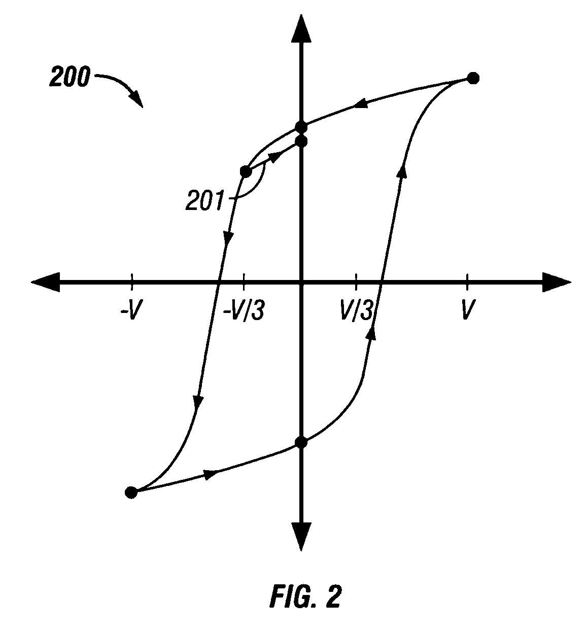
It would be difficult to store more than one bit per
cell in MRAM due to the squareness of the MTJ
hysteresis loop.
The complexity and cost of connecting three devices in series for storing twice as much
information needs further consideration.
A significant obstacle associated with MTJ-MRAM is that the current density necessary for producing a write field scales poorly as the wires are made smaller.
Consequently, the cost of MRAM will remain quite high in comparison to more scalable technologies.
Nevertheless, despite good 3-D potential, MRAM has poor scaling and does not appear competitive with other storage methods.
The primary disadvantages of Matrix memory are: (1) the memory is write-once because it is based on destructive breakdown of an insulator, and (2) the memory has low performance because a poly-
crystalline silicon diode is used.
If the number of grains or domain wall pinning sites is sufficiently large in a single
capacitor, it should be possible to store two or more bits per cell, but this should be difficult because the
intermediate state of the cell cannot be verified without destroying the state.

