Magnetoresistance effect element, magnetic head, magnetic reproducing apparatus, and magnetic memory

a technology of magnetoresistance and effect, which is applied in the field of magnetoresistance effect elements, magnetic reproducing apparatuses, and magnetic memory, can solve the problems of rapid decline difficult adoption from the viewpoint of shot noise and high frequency response, and disappearance of mr rate of change in this resistance level, etc., to achieve high sensitivity, high output, and stable obtained

Inactive Publication Date: 2007-11-27
KK TOSHIBA
View PDF18 Cites 54 Cited by
  • Summary
  • Abstract
  • Description
  • Claims
  • Application Information

AI Technical Summary

Benefits of technology

[0125]In order to acquire an effect of the invention fully, the structure where a very thin oxide layer exists in a magnetic layer film, or the structure where a very thin oxide layer exists in an interface with a spacer layer as shown in FIGS. 4 through 6 is more preferable than the structure of FIG. 7 where a very thin oxide layer exists in a position most distant from the spacer layer S. Structures shown in FIGS. 8 through 10 mentioned later are also more preferred than a structure shown in FIG. 11 by same reason. For example, as for a very thin oxide layer, it is desirable to be located within 3 nm from a non-magnetic spacer layer.
[0126]Moreover, the same effect is acquired by inserting the very thin oxide layer in a pin layer or a free layer. It is more effective to insert in a pin layer at this time than to insert in a free layer. That is because the magnetization response of the free layer may fall on device operation, when the very thin oxide layer is inserted in the interface or the inside of the free layer. In particular, this poses an essential problem, when providing the very thin non-magnetic layer NM in addition to the very thin oxide layer TB. And it becomes difficult to use it in and a free layer.
[0127]FIGS. 8 through 11 are principal part sectional views which illustrate structures where a metal magnetic layer FM is further provided between a very thin non-magnetic layer NM and a very thin oxide layer TB.
[0128]First, FIG. 8 expresses structure where a very thin oxide layer TB was inserted into a pinned layer P (or a free layer F). And a metal magnetic layer FM is laminated at the upper and lower sides of a very thin oxide layer TB, and a ferromagnetic layer is further laminated at the outside via a very thin non-magnetic layer. By providing such a magnetic layer FM, as mentioned above about FIG. 4, material which adjoins a very thin oxide layer TB is made to be changed suitably, and the band modulation effect of a very thin oxide layer TB can be emphasized.
[0129]In the case of this example, by inserting a metal magnetic layer FM, a magnetic effect in inside of a very thin oxide layer TB is assisted, and an effect which promotes magnetic coupling of a pinned layer P of the upper and lower sides through a very thin oxide layer TB (a free layer F) is acquired.
[0130]On the other hand, when a very thin oxide layer TB is formed by self-oxidization (or a self-nitride, self-fluoridation, etc.) of a metal layer, this metal magnetic layer FM may correspond to a portion which remained as that non-oxidized portion. In such a case, a laminated structure of a very thin oxide layer TB and a metal magnetic layer FM can be formed, keeping good the adjustment of an interface of a very thin oxide layer TB and a metal layer FM.

Problems solved by technology

However, in a TMR element, since the tunnel effect is used, when thickness of the non-magnetic intermediate layer made of alumina, for example, is made thin, there is a problem that MR rate of change decreases rapidly.
When application to a magnetic head is considered, its adoption is difficult from a viewpoint of a shot noise and a high frequency response.
However, in the case of a TMR element, there is a problem that MR rate of change disappears in this resistance level.
In the case of a TMR element, since an insulator is used for an intermediate layer, element resistance becomes high too much.
For this reason, if the miniaturization of the element area is carried out, originating in high resistance and causing shot noise generating peculiar to a tunnel phenomenon and high frequency response degradation will pose problems.
However, also in MRAM, the miniaturization of the element area is carried out with improvement in storage density, and it is expected that a problem that the resistance becomes too high comes out.
That is, also in any of a magnetic head and MRAM, high resistance peculiar to a TMR element poses a problem with improvement in storage density.
As a result, it is difficult to acquire a high reproduction output signal.
That is, compared with a case of the artificial lattice multilayer structure, thickness and interfaces which contribute to MR rate of change are both insufficient.
However, it is difficult to provide pinholes uniformly.
For this reason, fabrication of stable CPP elements is difficult.
Such an ideal state may be unable to be realized in fact.
However, if a difference of density of states of a up spin electron and a down spin electron becomes larger than conventional material, an increase of MR rate of change does not remain in improvement in about 2 times, but a rise of 3 times, 4 times, and still more nearly extraordinary fast MR rate of change is expected.
However, there is a big problem which obstructs utilization which is explained below in a half metal investigated intensively now.
Many of these materials have a complicated crystal structure.
There is a problem that these processes are not easy to carry out in a creation process of an actual magnetoresistance effect element.
This is the first problem.
However, there are the following problems as a still more essential problem.
Since temperature which shows half metal nature (here, it is defined as Thm) becomes the lower temperature side, there is a problem that material which shows half metal nature in room temperature is not yet found.
This is the second problem.
Thus, if half metal nature is realizable only at low temperature, the application to a consumer product is completely impossible.
However, with material investigated until now, Tc or Tn beyond room temperature hardly exists.
Intensive research is made in order to raise Tc and Tn, but a decisive solution which raises Tc or Tn in every material cannot be found.
That is, even if a half metal is realized in a single layer film, when it is provided in a multilayered structure like a spin valve, there is a problem that half metal nature in a laminated film interface is lost.
Although a half metal is realized in a single layer film, there is a problem that a half metal is unrealizable in an interface or the surface.
For this reason, it is very difficult for half metal nature to be made not to be lost in a junction interface.
When using these magnetic semiconductor material, it is desirable to also constitute a non-magnetic spacer layer from a semiconducting material, and the combination with metal material is not realistic.
Since half metal nature will be lost near the interface, it is meaningless to pursue material which half metal nature by using a single layer of a single crystal.
However, it is difficult to create the pinned layer, the spacer layer, and the free layer using material with a special crystal structure like perovskite.
And the above-mentioned second problem that Tc is low temperature is still not solved at all.
Thus, in extension of research of a half metal studied intensively now, realization of a high MR rate of change is difficult even in low temperature.

Method used


Image

  • Magnetoresistance effect element, magnetic head, magnetic reproducing apparatus, and magnetic memory
  • Magnetoresistance effect element, magnetic head, magnetic reproducing apparatus, and magnetic memory
  • Magnetoresistance effect element, magnetic head, magnetic reproducing apparatus, and magnetic memory

Examples


first example

[0185]The magnetoresistance effect element which has the following laminated structure was formed as the first example of the invention.

[0186]A lower electrode / tantalum (Ta) 3 nm / nickel iron chromium (NiFeCr) 5 nm / platinum manganese (PtMn) 10 nm / cobalt iron (CoFe) 4 nm / ruthenium (Ru) 0.9 nm / cobalt iron (CoFe) [4 nm / very thin oxide layer 0.5 nm / cobalt iron (CoFe) 1 mm / copper (Cu) 5 nm / cobalt iron (CoFe) 1 nm / nickel iron cobalt (NiFeCo) / copper (Cu)1 nm / tantalum (Ta)5 nm / upper electrode.

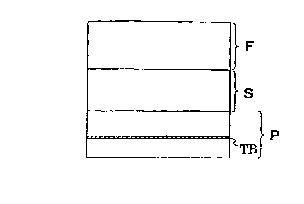
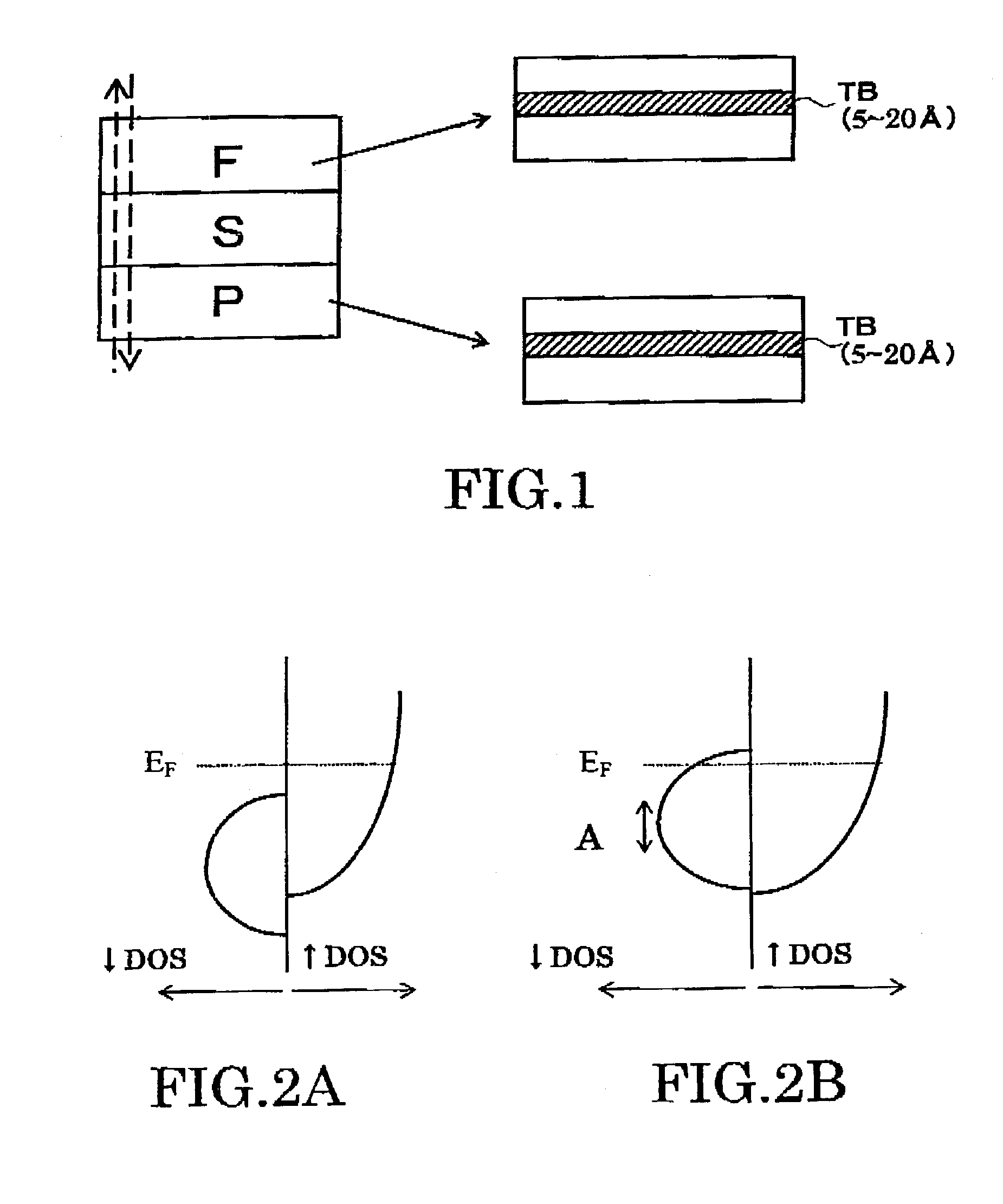
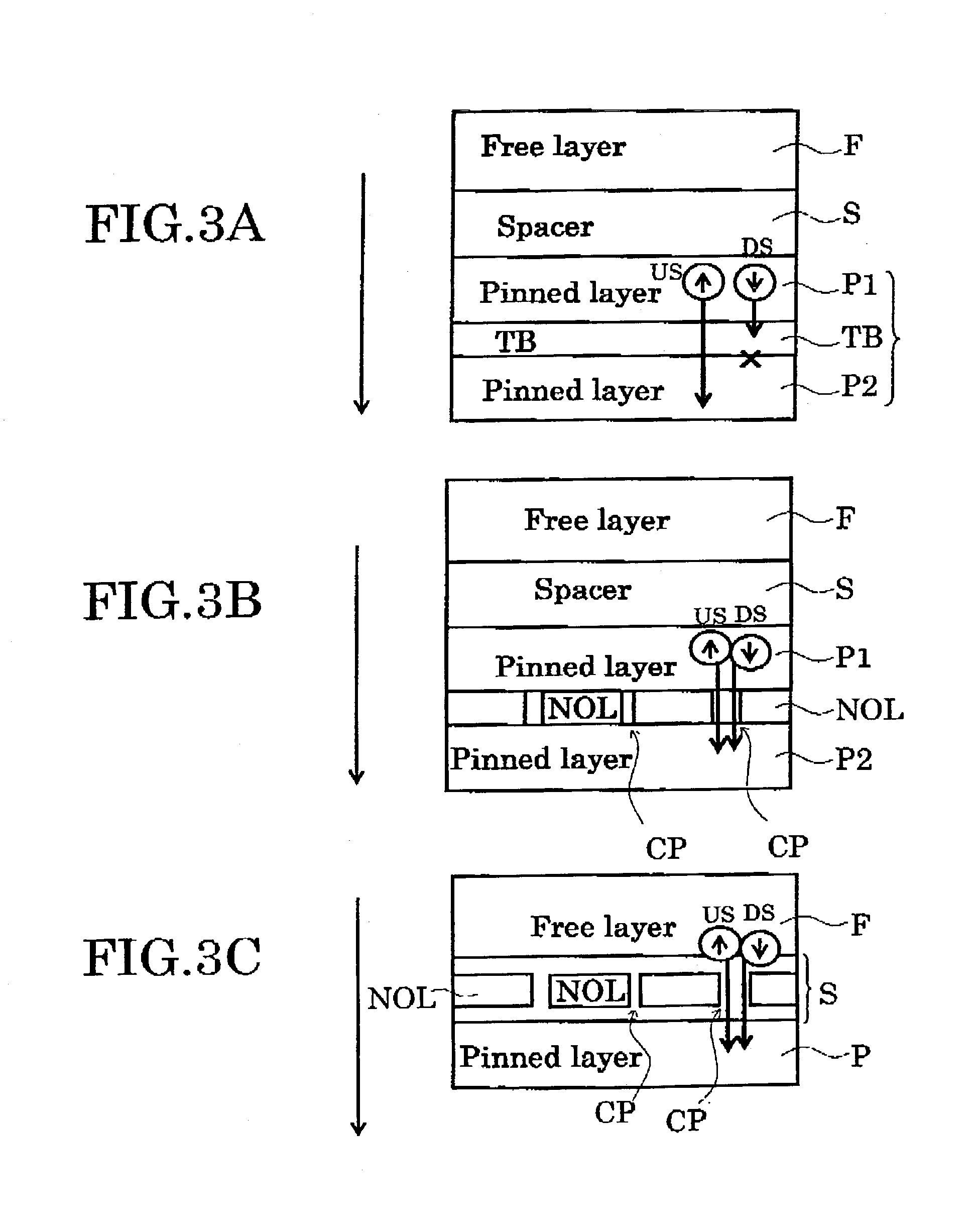
[0187]This example has structure where a very thin oxide layer TB is provided only near the interface with a spacer layer S of a pinned layer P, as shown in FIG. 14C.

[0188]In a case of this structure, 100 mΩμm2 to 200 mΩμm2 is obtained as AR, and 5 mΩμm2 to 30 mΩμm2 is obtained as AdR. Moreover, if the AR rise effect by the current constriction is combined, 500 mΩμm2 may be obtained as AR and 25 mΩμm2 to 150 mΩμm2 may be obtained as AdR, as will be explained later.

[0189]If a very thin oxide layer TB is ...

second example

[0271]Next, the example of the CPP type magnetoresistance effect element which can be used as a magnetic head is given and explained as the second example of the invention.

[0272]FIGS. 25 and 26 are conceptual diagrams which express typically the principal part structure of the magnetoresistance effect element concerning the embodiment of the invention. That is, these figures express the state where the magnetoresistance effect element is included in the magnetic head. FIG. 25 is a sectional view of the magnetoresistance effect element cut in parallel to the medium facing surface P which is opposite to a magnetic recording medium (not shown). FIG. 26 is a sectional view of the magnetic resistance effect element cut in the perpendicular direction to the medium opposite side P.

[0273]The magnetoresistance effect element illustrated in FIGS. 25 and 26 has a hard abutted structure. The lower electrode 2 and the upper electrode 6 are provided in the upper and lower sides of the magnetoresi...

third example

[0278]Next, a magnetic reproducing apparatus having inboard the magnetoresistance effect element of the embodiment will be explained as the third example of the invention.

[0279]That is, the magnetoresistance effect element or the magnetic head explained with reference to FIGS. 1 through 26 can be incorporated in a recording / reproducing magnetic head assembly and mounted in a magnetic reproducing apparatus.

[0280]FIG. 27 is a perspective view that shows outline configuration of this kind of magnetic reproducing apparatus. The magnetic reproducing apparatus 150 shown here is of a type using a rotary actuator. A magnetic reproducing medium disk 200 is mounted on a spindle 152 and rotated in the arrow A direction by a motor, not shown, which is responsive to a control signal from a controller of a driving mechanism, not shown. The magnetic reproducing apparatus 150 shown here may have a plurality of medium disks 200 inboard.

[0281]The medium disk 200 may be of a “lateral recording type” i...


PUM

PropertyMeasurementUnit
thicknessaaaaaaaaaa
orientation dispersion angleaaaaaaaaaa
sizeaaaaaaaaaa

Abstract

A magnetoresistance effect element comprises a magnetoresistance effect film and a pair of electrode. The magnetoresistance effect film having a first magnetic layer whose direction of magnetization is substantially pinned in one direction; a second magnetic layer whose direction of magnetization changes in response to an external magnetic field; a nonmagnetic intermediate layer located between the first and second magnetic layers; and a film provided in the first magnetic layer, in the second magnetic layer, at a interface between the first magnetic layer and the nonmagnetic intermediate layer, and / or at a interface between the second magnetic layer and the nonmagnetic intermediate layer, the film having a thickness not larger than 3 nanometers, and the film has as least one selected from the group consisting of oxide, nitride, oxinitride, phosphide, and fluoride. The pair of electrodes are electrically connected to the magnetoresistance effect film to supply a sense current perpendicularly to a film plane of said magnetoresistance effect film.

Description

CROSS-REFERENCE TO RELATED APPLICATIONS[0001]This application is based upon and claims the benefit of priority from the prior Japanese Patent Application No. 2002-092998, filed on Mar. 28, 2002, and the prior Japanese Patent Application No. 2002-263251, filed on Sep. 9, 2002; the entire contents of which are incorporated herein by reference.BACKGROUND OF THE INVENTION[0002]This invention relates to a magnetoresistance effect element, a magnetic head, a magnetic reproducing apparatus, and a magnetic memory and more particularly, to a magnetoresistance effect element which has a structure where a sense current is passed perpendicularly to a film plane of the magnetoresistance effect film, and to a magnetic head using the same, a magnetic reproducing apparatus and a magnetic memory.[0003]By discovery of the Giant MagnetoResistance effect (GMR) in the laminated structure of magnetic layers, the performance of a magnetic device, especially a magnetic head is improving rapidly. Especially...

Claims


Application Information

Patent Timeline
Patent Type & Authority Patents(United States)
IPC IPC(8): G11B5/33G11B5/127G11B5/39G01R33/09H01F10/16H01L21/8246H01L27/105H01L27/22H01L43/08H01L43/10
CPCB82Y25/00G01R33/093G11B5/3906G11B5/398G11B5/3983G11C11/16H01F10/1936H01F10/3281H01F41/303H01L43/08H01F10/3259H01F41/325B82Y40/00Y10T428/1121H01F10/3254H01F10/3268H01L27/224H01L27/228G11C11/161H10B61/10H10B61/22H10N50/10
Inventor FUKUZAWA, HIDEAKIYUASA, HIROMIFUKE, HIROMIIWASAKI, HITOSHISAHASHI, MASASHI
Owner KK TOSHIBA
Why Eureka
Try Eureka