
Diamond-coated electrode and method for producing same

a technology of diamond coating and electrode, which is applied in the direction of solid-state diffusion coating, plasma technique, natural mineral layered products, etc., can solve the problems of inability to raise the doped amount, the potential window is smaller, and the durability of diamond electrodes is not adequate, so as to achieve good anti-pealing strength, good film adhesion, and low resistance

Inactive Publication Date: 2008-01-01
SUMITOMO ELECTRIC IND LTD
View PDF13 Cites 11 Cited by
  • Summary
  • Abstract
  • Description
  • Claims
  • Application Information

AI Technical Summary

Benefits of technology

The present invention provides a method for manufacturing a conductive diamond electrode with good adhesion between the diamond film and substrate, low resistance, and high performance. The method involves raising the anti-pealing-off strength during electrolysis and increasing adhesion between the diamond film and substrate. The electrode has a substrate coated with diamond, which contains boron, and the concentration of boron is at least 10,000 ppm and no more than 100,000 ppm. The diamond is polycrystalline CVD diamond with a coefficient of thermal expansion of the substrate within a limited range. The method also involves adding nitrogen, tungsten, or tungsten carbide during diamond production to prevent loss of crystallinity and improve the stability of the diamond film. The electrode can be used to decompose a substance in a solution through an electrochemical reaction.

Problems solved by technology

1-4” states that when an electrolysis test is performed using a conductive diamond film formed on a silicon substrate or niobium substrate, a diamond electrode may not have adequate durability due to separation of the diamond film or corrosive wear of the substrate, depending on the solution or electrolysis conditions.
In a method in which trimethyl borate is doped with a filament CVD, it has been indicated that doping a large quantity of boron makes the potential window smaller, so the doped amount cannot be raised.
The same thing has been mentioned in Patent Document 2, which states that the doping a large quantity of boron adversely affects diamond film quality and prevents the properties inherent in diamond from being obtained.
Thus, existing methods have had a number of problems in terms of stably producing low-resistance conductive diamond by doping a large quantity of boron to a diamond electrode with a large surface area, and making the substrate thereof sufficiently durable.

Method used


Image

  • Diamond-coated electrode and method for producing same
  • Diamond-coated electrode and method for producing same
  • Diamond-coated electrode and method for producing same

Examples


example 1

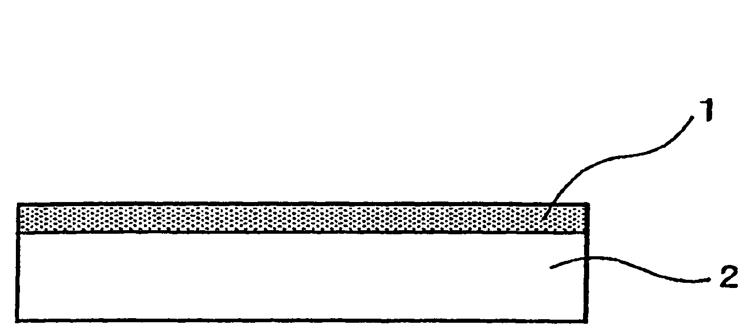
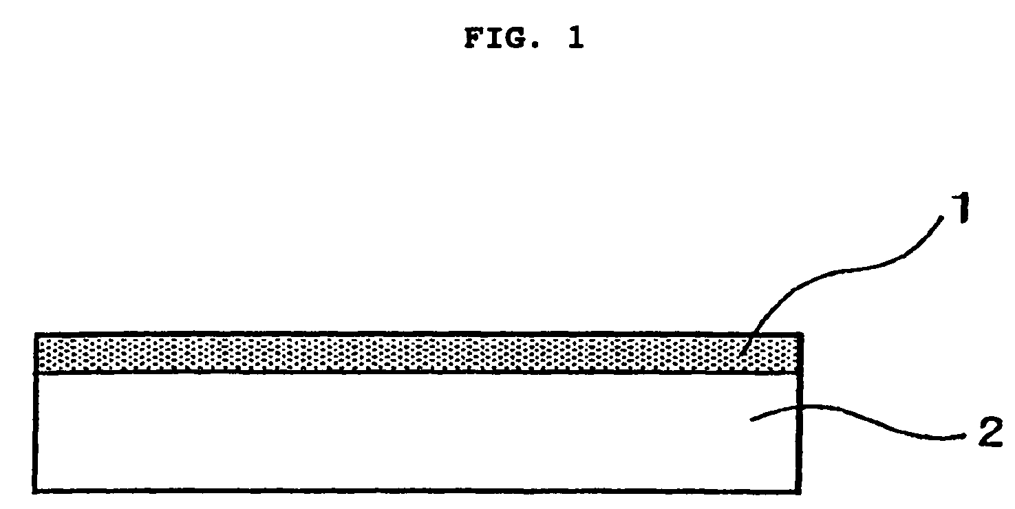
[0070]Substrates of the size and material shown in Table 1 were used as a base material, and the surface thereof was scratched with diamond powder and then washed. Each of these substrates was placed in the synthesis apparatus shown in Table 1, and conductive diamond 1 was synthesized on the base material 2 as shown in FIG. 1.

[0071]As shown in Table 1-1, the synthesis was conducted at a gas pressure of 2.7 kPa or 7 kPa, a hydrogen flow of 5000 sccm, and a methane (CH4) flow range of 0.5 to 2.0 sccm. Triethyl borate [B(OC2O5)3] was used as a boron source. Argon gas was bubbled in as a carrier gas, and boron was supplied at a concentration range of 0.2 to 1.0% in atomic ratio with respect to carbon. The temperature of the substrate that is a base material was between 700 and 1000° C.

[0072]When the synthesis apparatus was a hot filament CVD apparatus (HFCVD), the filament was made of tungsten and the filament temperature was between 2000 and 2200° C. When the synthesis apparatus was a ...

example 2

[0080]Substrates of the various types and in the states of working shown in Table 2-1 were subjected to seeding with diamond powder in advance, after which a hot filament CVD apparatus was used to form a diamond film on each under several varieties of formation conditions (sample Nos. 2-1 to 2-20). The size of each substrate was 60 mm square, and the thickness was 2 mm. The coefficient of thermal expansion of each substrate was the average coefficient of thermal expansion within 40-800° C. The gases used here were introduced into the apparatus by bubbling argon through a bubbler, which was filled with H2, CH4 and trimethyl borate [B(OC2O5)3] as a boron source.

[0081]The common conditions were kinds of gases, an H2 flow of 1000 sccm, a CH4 flow of 20 sccm, and an Ar+B(OCH3)3 flow of 5 sccm, the use of a tungsten filament with a diameter of 0.2 mm, a filament temperature of 2200° C., and a substrate-filament spacing of 5 mm. The substrate temperature was adjusted to within 600-950° C. ...

example 3

[0090]Another experiment was conducted by using the substrates in Example 2 (sample Nos. 2-11, 12, 14, 16, and 17) and changing the conditions of the electrolysis test. The electrolysis test was conducted under the conditions: for 1000 hours using a 0.1M sodium sulfuric acid solution, at an electric current density of 1.0 A / cm2, and using the same type of electrode for both electrodes. The results are given in Table 3.

[0091]It can be seen from Table 3 that, with sample Nos. 2-12′ and 2-17′, which had the surface of a ceramic substrate worked after sintering, separation occurred in Example 3 that set the harsher conditions although no separation occurred in the electrolysis test of Example 2.

[0092]In contrast, no separation occurred in Nos. 2-11′, 2-14′ and 2-16′, which had the surfaces worked prior to sintering, even in the electrolysis test of Example 3.

[0093]Also, when the same substrate as 2-17′, which separated under the Example 3's conditions, was used and when the substrate wa...


PUM

PropertyMeasurementUnit
surface roughnessaaaaaaaaaa
thicknessaaaaaaaaaa
thicknessaaaaaaaaaa

Abstract

A diamond electrode having a sufficiently low resistance is disclosed which is realized by increasing the amount of boron added thereto. A method for producing a high-performance, high-durability electrode is also disclosed by which adhesiveness between a diamond coating and a substrate and separation resistance during electrolysis are sufficiently increased. An electrode composed of a substrate and a diamond layer coating the substrate is characterized in that the electrode is composed of a base coated with diamond and the diamond contains boron in such an amount that the boron concentration is not less than 10,000 ppm but not more than 100,000 ppm. The base is preferably made of an insulating material.

Description

BACKGROUND ART[0001]Diamond by vapor phase synthesis is known as a way to obtain polycrystalline diamond with a relatively large surface area less expensively than natural diamond or manmade monocrystalline diamond obtained under ultra-high pressure, and such diamond is utilized in optical component applications and as heat sinks for electronic components and tools. Known film formation methods include microwave plasma CVD, hot filament CVD, DC arc jet plasma CVD, and so forth. Diamond obtained by these methods usually exhibits electrically insulating property, but can be rendered conductive by doping impurities during the film formation. Such conductive diamond has for some time been the subject of research and development in semiconductor and electronic component applications, particularly in the growth of monocrystalline diamond in the vapor phase, but imparting conductivity to polycrystalline diamond produced by vapor phase synthesis has been attracting particular attention in r...

Claims


Application Information

Patent Timeline
Patent Type & Authority Patents(United States)
IPC IPC(8): C25B11/12C02F1/461C25B11/04
CPCC02F1/46109C25B11/0442C02F2001/46133Y10T428/30C02F2001/46138C25B11/073C25B11/052
Inventor SEKI, YUICHIROIZUMI, KENJIIMAI, TAKAHIRO
Owner SUMITOMO ELECTRIC IND LTD
Learn More