

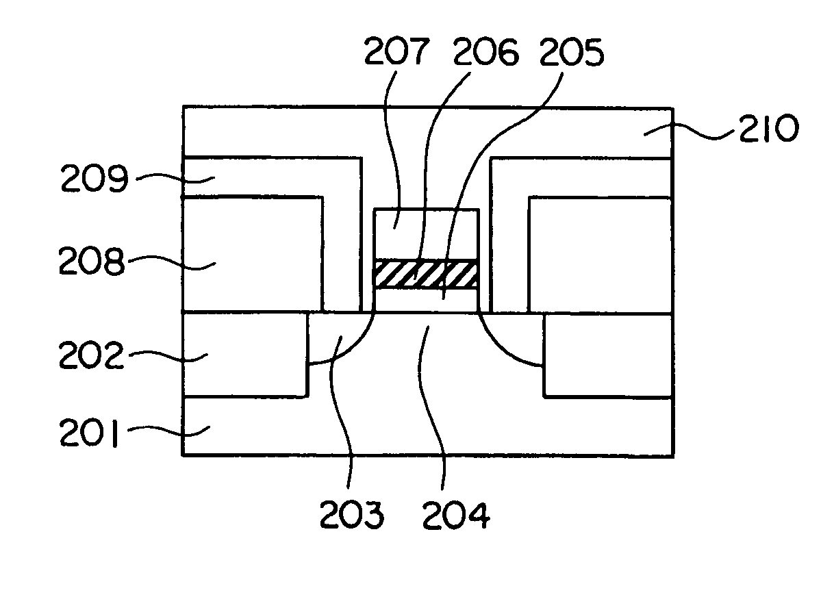
High dielectric constant MOSFET device
a dielectric constant and mosfet technology, applied in the field of high dielectric constant mosfet devices, can solve the problems of high possibility of deterioration in performance of transistors, variations in characteristics, and inability to use silicon oxide films, and achieve the effects of preventing the formation of fixed charges due to nitriding of silicon substrates, high plasma reactivity, and high voltag
- Summary
- Abstract
- Description
- Claims
- Application Information
AI Technical Summary
Benefits of technology
Problems solved by technology
Method used
Image

Examples
first embodiment
[0079]In the first embodiment, an aluminum oxynitride film was deposited on a silicon substrate by reactive sputtering. A magnetron sputtering apparatus was used as a reactive sputtering apparatus. An n-type silicon substrate (100) was used as a substrate. Aluminum was used as a target, the distance between the target and the substrate was controlled at about 10 cm, and reactive sputtering was carried out, so as to form an aluminum oxynitride thin film of 5 nm in thickness. The pressure in a chamber was 5×10⁻⁵ Pa when the sputtering was not carried out.
[0080]An oxygen-nitrogen mixed gas was supplied during the film formation. Preferably, the total pressure of the mixed gas is controlled at a such level that the mean free path of the gas becomes in the order of a fraction of the distance between the target and the wafer to reduce implantation of sputtered particles into the substrate. The mean free path L (cm) of the gas is represented by L=1.33 / P where a pressure is P (Pa). Preferab...
second embodiment
[0084]The second embodiment is almost the same as the first embodiment except that a first insulating film is provided between the silicon substrate and the aluminum oxynitride and a laminated film was thereby prepared. The second embodiment is different from the first embodiment in the point that an n-type silicon substrate (100) with 0.5 nm of silicon oxide film (the first insulating film) is used as the substrate.
[0085]Aluminum was used as a target, the distance between the target and the substrate was controlled at about 10 cm, and reactive sputtering was carried out, so as to deposit an aluminum oxynitride thin film of 5 nm in thickness. The pressure in a chamber was 5×10⁻⁵ Pa when the sputtering was not carried out. An oxygen-nitrogen mixed gas was supplied during the film formation, the pressure in the chamber was controlled at 0.6 Pa, and the power of the high frequency of the RF power supply (frequency 13.56 MHz) was 500 W. In order to compensate oxygen vacancies, annealing...
third embodiment
[0096]In the third embodiment, aluminum oxynitride was formed by an atomic layer deposition method (ALD method). FIG. 6 shows a conceptual diagram of an atomic layer deposition apparatus with a plasma source, used in the present embodiment. The present apparatus is composed of a sample treatment chamber 101 and an exchange chamber 102, and a plurality of wafers 103 can be contained in the exchange chamber 102. A gate valve 104 is provided between the sample treatment chamber 101 and the exchange chamber 102, and gases are exhausted from the chambers with exhaust systems 105 and 106, respectively, composed of a plurality of pumps.
[0097]A heater 107 is disposed immediately below a wafer 108 carried from the exchange chamber to the sample treatment chamber, and heats the wafer to a predetermined temperature. An ECR plasma source 109 is disposed above the wafer 108 in the upper portion of the chamber, and serves as a plasma source.
[0098]In order to form a metal oxynitride on the upper s...
PUM
 Abstract
Description
Claims
Application Information