
Method of producing a device with a movable portion

a technology of movable parts and devices, applied in the field of micro optoelectromechanical devices, to achieve the effect of improving the surface condition of devices, improving the planarity of surfaces, and improving the device fabrication process

Active Publication Date: 2008-07-08
FRAUNHOFER GESELLSCHAFT ZUR FOERDERUNG DER ANGEWANDTEN FORSCHUNG EV
View PDF15 Cites 13 Cited by
  • Summary
  • Abstract
  • Description
  • Claims
  • Application Information

AI Technical Summary

Benefits of technology

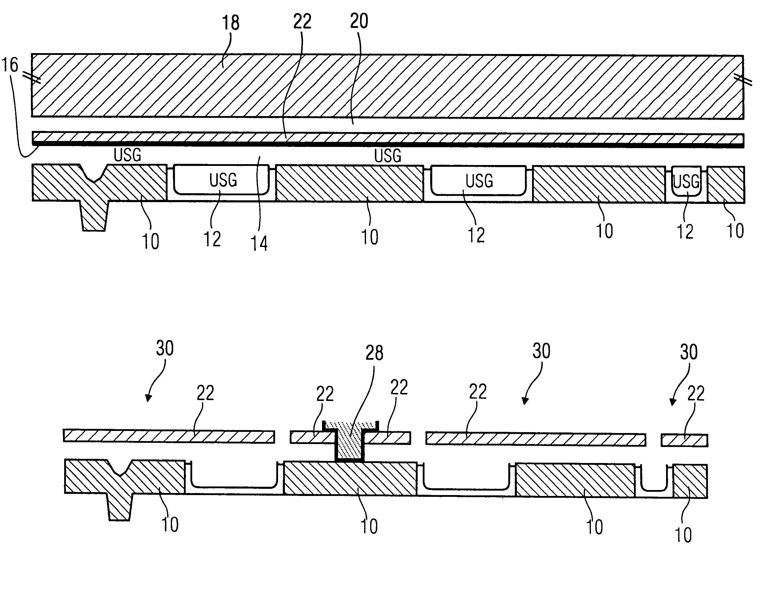
The present invention provides a method for producing a spatial light modulator with improved properties compared to conventional methods. The method involves using a support wafer with a structured surface and a device wafer with a backing layer and a device layer. The method includes generating a first planarization layer on the support wafer to fill in the structures of the surface, and a second planarization layer on the first planarization layer to achieve a higher degree of planarization. The device wafer is then bonded onto the planarized surface of the support wafer, and the backing layer is removed. The resulting structure is then structured and the first and second planarization layers are removed to create the moveable portion of the device. The use of a silica glass-based material for both planarization layers allows for improved surface condition and reduced stress load on the device layer. The method is cost-effective and efficient for producing such devices.

Problems solved by technology

The conventional and currently used SLM technology based on aluminum mirrors has certain limitations or constraints in this regard.
Although it is possible to obtain a fairly homogeneous thin film with minor stress gradients, the alloy is subject to re-crystallization and stress relaxation upon heating and also sensitive to mismatch in contrast to the surrounding material, such as the spacer, during thermal expansion.
Small changes in the crystal structure lead to stress gradients in the thin film that easily warps of deforms a micromirror made out of such an alloy.
Thereby, it is extremely difficult to obtain a good mirror planarity.
The statistical nature of the material itself as well as changes in the process conditions inevitably lead to a limited reproducibility and also, to a certain amount, to a dependency on a statistical spread of the planarity, so that it is impossible to perform an exact control and reproducibility of the planarity.
Otherwise, the wafer-to-wafer and run-to-run reproducibility is limited.
Further, an aluminum alloy is susceptible to plastic deformation upon bending.
In that way, the mirror planarity can change during use, which limits the life span of such an SLM.
However, up to now, such thin silicon membranes has not been successfully bonded to CMOS wafer, and thus the prior art has clear limits.
With regard to “flip chip” bonding of structured micromirrors (U.S. Pat. No. 6,587,613 B1, U.S. Pat. No. 6,800,210 B2 or U.S. Pat. No. 6,798,561 B2) it has to be said that this bonding requires a highly accurate alignment of the mirror structure with regard to the control electronics and that further the conditions for alignment accuracy increase rapidly with reduction of the pixel size, thus the method has limited scalability.
With regard to the layer transfer of monocrystalline silicon by eutectic bonding (WO 03 / 068669 A1) it has to be mentioned that this bonding of the wafers is based on forming an eutectic gold silicon alloy, which requires temperatures in excess of 363° Celsius and thus means a risk for increased stress in the transferred film.
A further disadvantage is that an indiffusion of gold has to be performed, which can affect the mechanical performance of nearby elements, such as mirror hinges.
Additionally, locally limited stress can be built up and crystal defects can occur at the bonded areas, which are sources for crack formation during thinning down.
This is particularly a problem when very thin films, such as are required for spatial light modulators, have to be bonded.
While this method of eutectic bonding has the advantage of being able to produce electrical and mechanical connections between mirrors and electronics directly without further processing (i.e. no filling elements are used), there is a disadvantage in that the area where bonding is performed is limited and in direct conflict to the requirement for compact post structures.
Further, it has to be mentioned about eutectic bonding that it requires that a contact between post and film is achieved on all locations on the film, which is, however, very difficult, sincea) there are slight variations of the post heights, andb) the mating wafers (i.e. the SOI wafer and the wafer providing the control electronics) have variations in thickness.
Thereby, the difficulty is the strength of the wafers and the structures on the wafers, whereby bonding becomes sensitive to local height variations.
In relation to a layer transfer of a monocrystalline silicon by adhesive bonding (according to the above-mentioned disclosure of F. Niklaus, S. Haasl and G. Stemme) it has to be mentioned that this adhesive bonding has a limited bonding strength, caused by the dependence of the adhesive capability of the used adhesive material.
As long as no specific precautions are taken, the gap between the bonded wafers will be non-uniform and structure-dependent.
Further, it is a disadvantage of adhesive bonding that outgassing can occur during bonding, which leads to the formation of bubbles.
Further, it has to be mentioned that there is a risk of particle contamination prior to bonding caused by the lack of suitable bonding tools allowing cleaning immediately prior to bonding as a partial step of the bonding process.
Further, it is a disadvantage of adhesive bonding that temperature limitations occur due to material instability, such as material flow or decomposition at elevated temperatures, which might exclude the usage of W-CVD (W-CVD=tungsten based chemical vapor deposition) for forming the planar surface after bonding.
Further, it has to be mentioned that non-ideal material properties, such as sodium contamination of certain polymers cause incompatibility with CMOS electronics or with standard microfabrication processes.
Further, the above-mentioned patent application remains non-specific about how a thin film is to be deposited on the electronic substrate.
Additionally, no direct information is given on how this is to be performed particularly with a monocrystalline silicon thin film.
The disclosure in the above-mentioned patent application that thinning down of part of the silicon wafer can be performed (such as disclosed on page 3 and 7 of the mentioned patent application), would cause problems when the goal is a 300 nm thick membrane, since the accuracy of such a process is very poor.

Method used


Image

  • Method of producing a device with a movable portion
  • Method of producing a device with a movable portion
  • Method of producing a device with a movable portion

Examples


Embodiment Construction

[0026]In the accompanying figures, equal or similar elements are provided with the same or similar reference numbers, whereby a repeated description of these elements has been omitted.

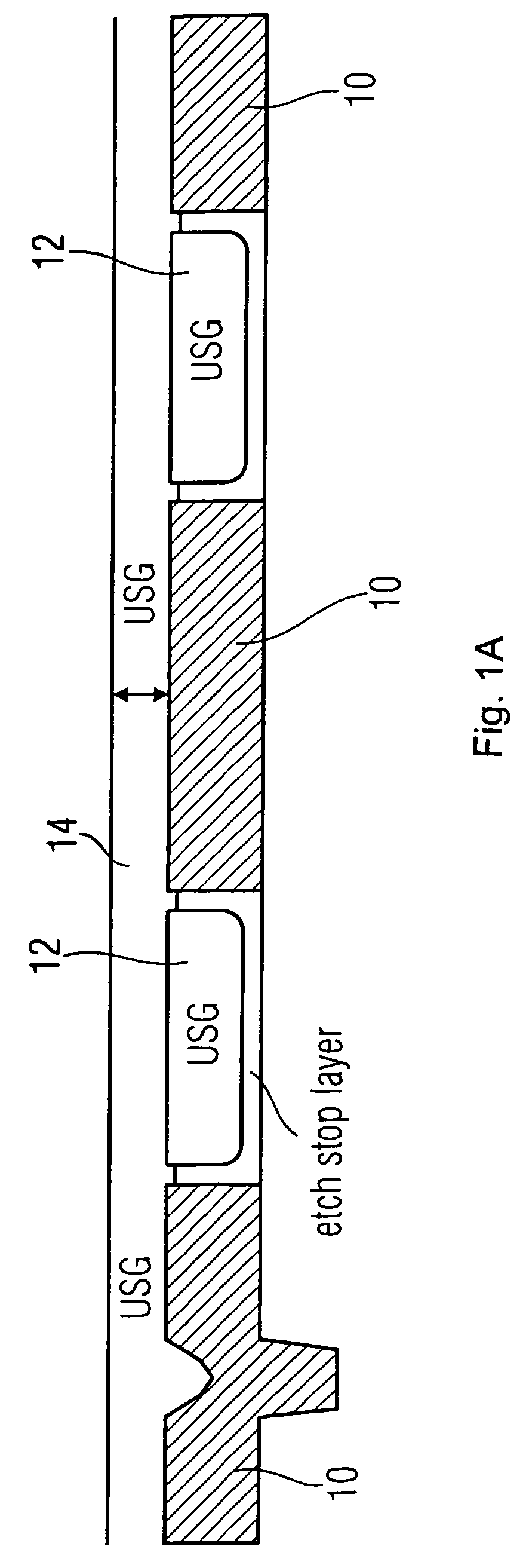
[0027]Direct bonding via an interface layer of, for example, spin on glass enables a very strong connection with excellent long term stability. The main difficulty is to achieve a sufficiently smooth and planar surface. Generally, bonding can be achieved when the RMS surface roughness (RMS=root mean square) is better than 0.5 nanometers. First, the CMOS wafer is planarized, for example by using an oxide CMP method (CMP=chemical mechanical polishing), such as illustrated in FIG. 1A. The planarization is a two step process, where 1 μm thick electrodes 10 are first covered by a thick layer 12 of undoped silica glass USG (USG=undoped silica glass) deposited by PECVD (PECVD=plasma enhanced chemical vapor decomposition), which can then be polished back (for example onto the electrode surface). The residual n...


PUM


Abstract

A method of producing a device with a movable portion spaced apart from a support wafer comprises a step of providing the support wafer having a structured surface and a further step of providing a device wafer with a backing layer and a device layer disposed thereon. Further, the method comprises the step of generating a first planarization layer from a first starting material on the support wafer with a first method to fill in the structures of the structured surface of the support wafer, whereby a surface with a first degree of planarization is obtained. Further, the method comprises a step of generating a second planarization layer from a second starting material on the planarized surface of the support wafer with a second method to obtain a surface with a second degree of planarization, which is higher than the first degree of planarization, wherein the first and second planarization layers can be removed together. Additionally, the support wafer is connected to the device wafer such that the device layer and the planarized surface of the support wafer are connected. Then, removing the backing layer of the device wafer is performed, followed by structuring the resulting structure and removing the first and second planarization layers via a common method to generate the moveable portion of the device.

Description

CROSS-REFERENCE TO RELATED APPLICATION[0001]This application claims priority from German Patent Application No. 102005002967.1, which was filed on Jan. 21, 2005 and is incorporated herein by reference in its entirety.BACKGROUND OF THE INVENTION[0002]1. Field of the Invention[0003]The present invention relates to the technical field of micro optoelectromechanical devices (MOEMS devices) and particularly, the present invention relates to the technical partial field of spatial light modulators on a semiconductor wafer.[0004]2. Description of the Related Art[0005]Spatial light modulators, also referred to as SLM, which are based on micromirrors for optical lithographic applications, require an exceptionally high mirror planarity to provide a tool having a high lithographic resolution and a dimensional or scalar uniformity. The conventional and currently used SLM technology based on aluminum mirrors has certain limitations or constraints in this regard. This technology is based on produc...

Claims


Application Information

Patent Timeline
Patent Type & Authority Patents(United States)
IPC IPC(8): H01L21/30H01L21/311H01L21/316
CPCB81C1/00142G02B26/0833B81C1/00611B81B2201/042B81C2201/0121B81C2201/019
Inventor BAKKE, THORFRIEDRICHS, MARTINVOLKER, BENJAMINHAASE, THOMAS
Owner FRAUNHOFER GESELLSCHAFT ZUR FOERDERUNG DER ANGEWANDTEN FORSCHUNG EV
Learn More