Thin film coated microwell arrays and methods of using same

a microwell array and thin film technology, applied in the field of microwell array compositions, can solve the problems of low sensitivity, lack of reproducibility, and high background signal

Inactive Publication Date: 2010-03-23
454 LIFE SCIENCES CORP
View PDF21 Cites 61 Cited by
  • Summary
  • Abstract
  • Description
  • Claims
  • Application Information

AI Technical Summary

Benefits of technology

[0158]As illustrated above, one particular advantage of the present invention is that, particularly through the use of fiber optic technology, improved extremely high density arrays can be made. Thus, for example, it is possible to have as many as 50,000 different fibers and cells in a 1 mm2 fiber optic bundle, with densities of greater than 250,000 individual fibers per 0.5 cm2 obtainable.
[0159]For example, a wide channel reaction chamber can have dimensions of approximately 14 mm×43 mm. Thus, with this approximate dimension and at approximately 4.82×10⁻⁴ chambers / um2 density, the array can have approximately 290,000 reaction chambers.
[0160]Reaction chambers are formed in the surface of the substrate as is generally known in the art using a variety of techniques, including but not limited to, chemical etching, photolithography, stamping techniques, pressing, casting, molding, microetching, electrolytic deposition, chemical or physical vapor deposition employing masks or templates, electrochemical machining, laser machining or ablation, electron beam machining or ablation, and conventional machining. The technique will depend on the composition and shape of the substrate. In one embodiment, reaction chambers are formed using chemical etching. Reaction chambers are typically formed in the substrate prior to coating the array with any thin film coating.
[0162]The present invention provides for the application of one or more thin film coatings to the array substrate. A thin film coating is a transparent or a non-transparent coating. Such transparent and non-transparent thin film coatings are designed to improve the properties and functions of the array, including to improve the compatibility of the reaction mixture or assay solution with the array substrate and to reduce problems such as optical bleed and physical interference between neighboring reaction chambers. The transparent thin film coating provides a barrier between the solution contained in the reaction chamber and the substrate and prevents both leaching of the substrate material into the solution and contact between the contents in the reaction chamber and the substrate. The non-transparent thin film coating provides a photon barrier which prevents the leaking of photons from one reaction chamber into another adjoining reaction chamber (i.e. cross-talk). The non-transparent coating creates a barrier which does not permit light to pass between neighboring reaction chambers and thus, restrains the photons and keeps the light in the reaction chamber to eliminate optical scattering. A non-transparent coating can be used to improve the retention of beads or particles in the reaction chamber (e.g., solid-support beads for carrying out a chemical reaction).
[0163]The thin film coatings of the present invention are typically applied to coat the bottom or sidewall of the reaction chambers or the top surface of the array. For the purposes of this invention, when a bottom or sidewall of the reaction chamber or the top surface of the array is coated with a thin film coating, the coating partially, substantially, or completely covers the surface of the bottom, sidewall or top surface. In one embodiment, the bottom, sidewall, or top surface is completely covered when the surface of the bottom, sidewall, or top surface is covered 100% with the thin film coating. In another embodiment, the bottom, sidewall, or top surface is substantially coated when the surface of the bottom, sidewall, or top surface is covered 97-100% with thin film coating. In another embodiment, the bottom, sidewall, or top surface is partially coated when the surface of the bottom, sidewall, or top is covered less than 97% with thin film coating. In another embodiment, the bottom, sidewall, or top surface is partially coated when at least 80% of the bottom, sidewall, or top is covered with thin film coating. In another embodiment, the bottom, sidewall, or top surface is partially coated when at least 60% of the bottom, sidewall, or top is covered with thin film coating. In another embodiment, the bottom, sidewall, or top surface is partially coated when at least 40% of the bottom, sidewall, or top is covered with thin film coating. In another embodiment, the bottom, sidewall, or top surface is partially coated when at least 20% of the bottom, sidewall, or top is covered with thin film coating. In another embodiment, the bottom, sidewall, or top surface is partially coated when at least 10% of the bottom, sidewall, or top is covered with thin film coating.
[0164]In one aspect of the invention, the non-transparent coating is deposited on at least one bottom or sidewall of substantially all of the reaction chambers or top surface of the array. In another embodiment, the non-transparent coating is deposited on at least one bottom or sidewall of substantially all of the reaction chambers or top surface of the array, and the non-transparent coating is deposited on the array prior to a transparent coating being deposited on at least one bottom or sidewall of substantially all of the reaction chambers or top surface of the array. In another embodiment, a transparent coating is deposited on at least one bottom or sidewall of substantially all of the reaction chambers or top surface of the array, and the transparent coating is deposited on the array prior to a non-transparent coating being deposited on at least one bottom or sidewall of substantially all of the reaction chambers or top surface of the array.

Problems solved by technology

Although there are several types of microwell arrays available, many microwell materials prove to be incompatible with the components of bioassays and chemical reactions and result in problems such as low sensitivity, high background signal, and lack of reproducibility.
One major disadvantage of this type of fiber optic array is the constraint of the materials comprising the fiber optic bundle.
These fiber optic materials are often incompatible with many reaction conditions, particularly bioassays which are often conducted in aqueous solutions and contain sensitive enzymatic reagents.
Multivalent heavy metals, such as barium and lanthanum, can interact unfavorably with enzymes, especially those enzymes with metal ion co-factors.
All of these effects will tend to degrade the performance of assays and reactions conducted in the fiber optic reaction chambers.
Increasing miniaturization also tends to exacerbate these unfavorable effects.
The fact that the fiber optic substrate is comprised of two materials (core and cladding) also can limit the effectiveness of any surface modification of the reaction chambers with a monolayer (e.g. functional groups).
Thus, any modification of the fiber optic substrate with a single polyelectrolyte is impossible since the substrate does not contain a single uniform charge.
The optical properties of a fiber optic substrate are also limited.
These photons which travel through the transparent cladding are often referred to as optical scattering and result in problems such as optical bleeding and physical interferences (e.g., cross-talk) between neighboring reaction chambers.

Method used


Image

  • Thin film coated microwell arrays and methods of using same
  • Thin film coated microwell arrays and methods of using same
  • Thin film coated microwell arrays and methods of using same

Examples


example 1

General Etching Process and RER Cleaning Procedure

[0255]This example describes the general single-sided etching process for FOFs (Incom Corporation, Charlton, Mass.) sizes 25×75 mm or 40×75 using silicon etch gaskets and PEEK (Poly Ether Ether Ketone) plastic clamps (FIGS. 11a and 11b). Distilled water for the Branson Ultrasonic bath (Fischer Scientific, Hampton, N.H.), from a PicoPure™ water purification unit (“PicoPure water”), was degassed for 10 minutes. The NesLab recirculator (Portsmouth, N.H.) was set to 57.2° C. (at this setting, water inside the ultrasonic bath was maintained at a constant temperature of 55° C.). Four stainless steel containers were covered and placed in the ultrasonic bath. Each container was charged with 1000 mL (for a 25×75 mm FOF) and 1200 mL (for a 40×75 mm FOF) of 20% HNO3 and warmed to 55° C. Ninety-six unetched FOFs were loaded into each of the 96 positions of four etch trays. A designated FOF was selected and weighed. The difference in FOF weight b...

example 2

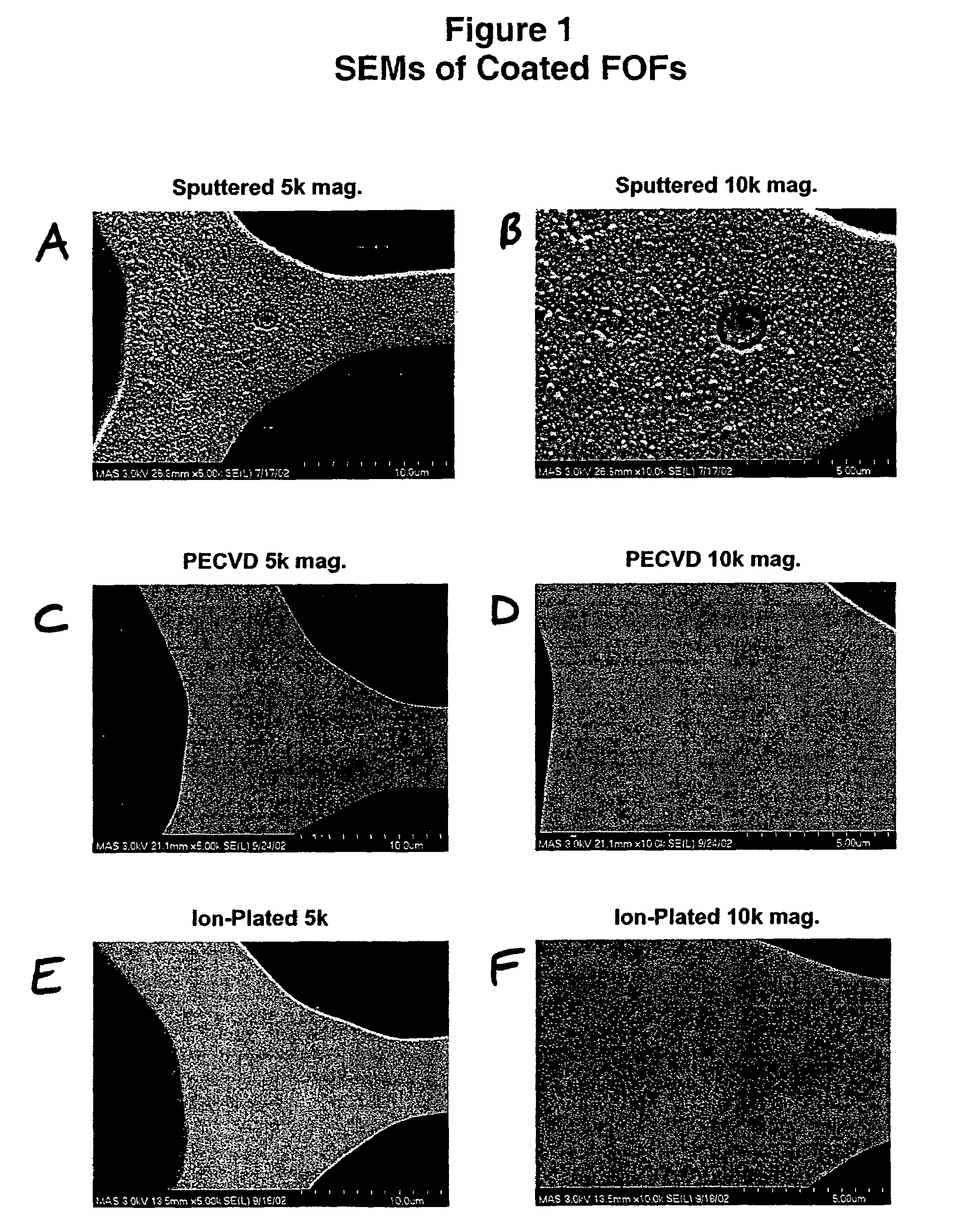
FOF Coating Using Ion-Plating Deposition Method

[0270]FOFs were immediately cleaned prior to thin film coating. The detergent used was Contrad®. The Branson sonicator was set to 40° C. Two FOFs were placed back to back in a Falcon tube, and 40-45 mL of 5% Contrad® solution was added in the tube and the cap closed. The tube was loaded in the sonicator and sonicated for 90 min. FOFs were removed from the tube, rinsed thoroughly with fresh deionized water, and transferred to a new Falcon tube and filled with deionized water. The detergent solution was disposed in the sink and FOFs kept in de-ionized water at 4° C.

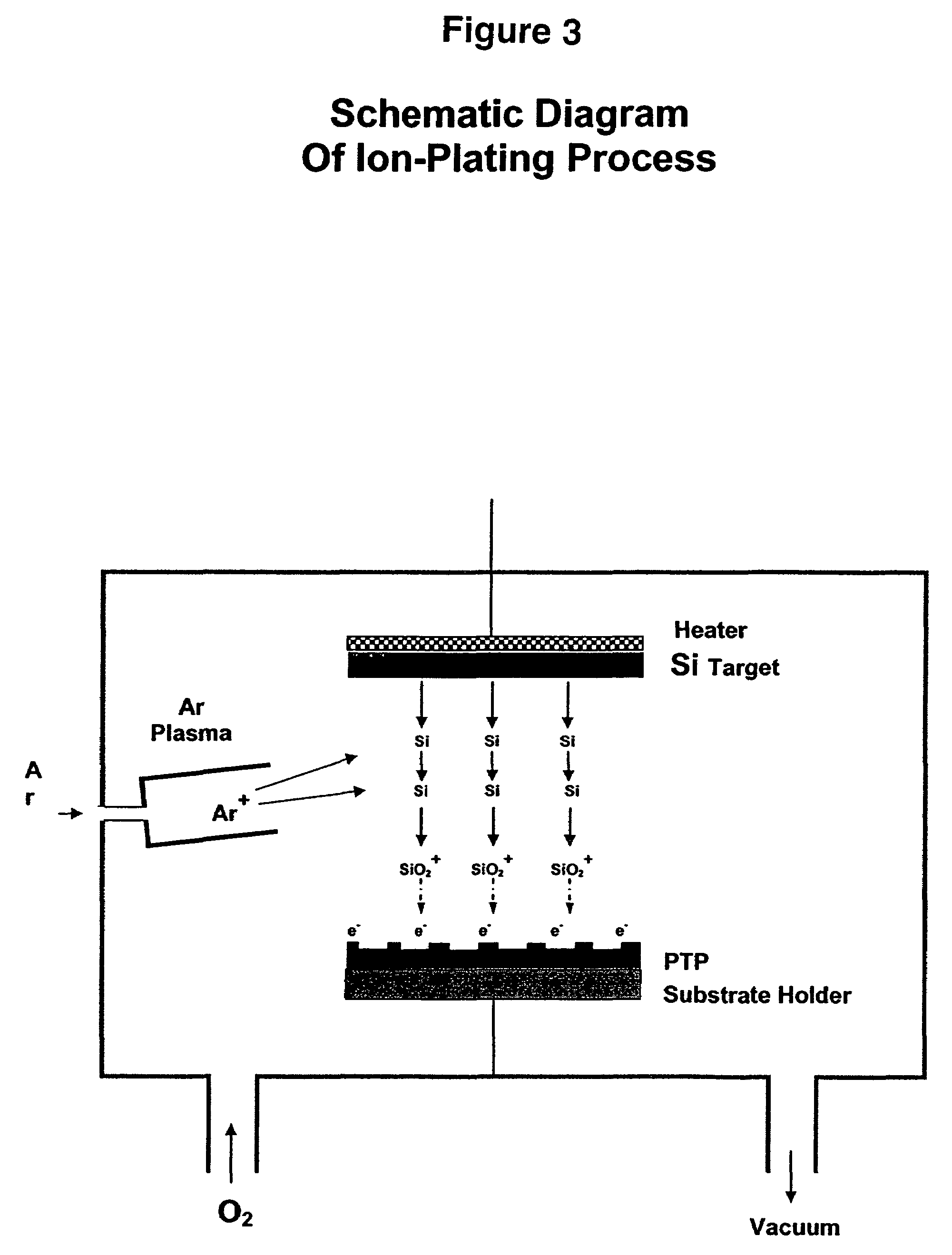
[0271]After cleaning, the ion-plating process for coating a chemically etched FOF with a thin film SiO2 coating was performed. The FOF to be coated was placed on an electrically isolated holder in a vacuum chamber, along with an electrically isolated heated silicon target, an argon plasma source, and a source of oxygen. The argon plasma source was ignited, which generated an ov...

example 3

Exposure of the Transparent Thin Film Coated FOF to “Mock” PCR Conditions

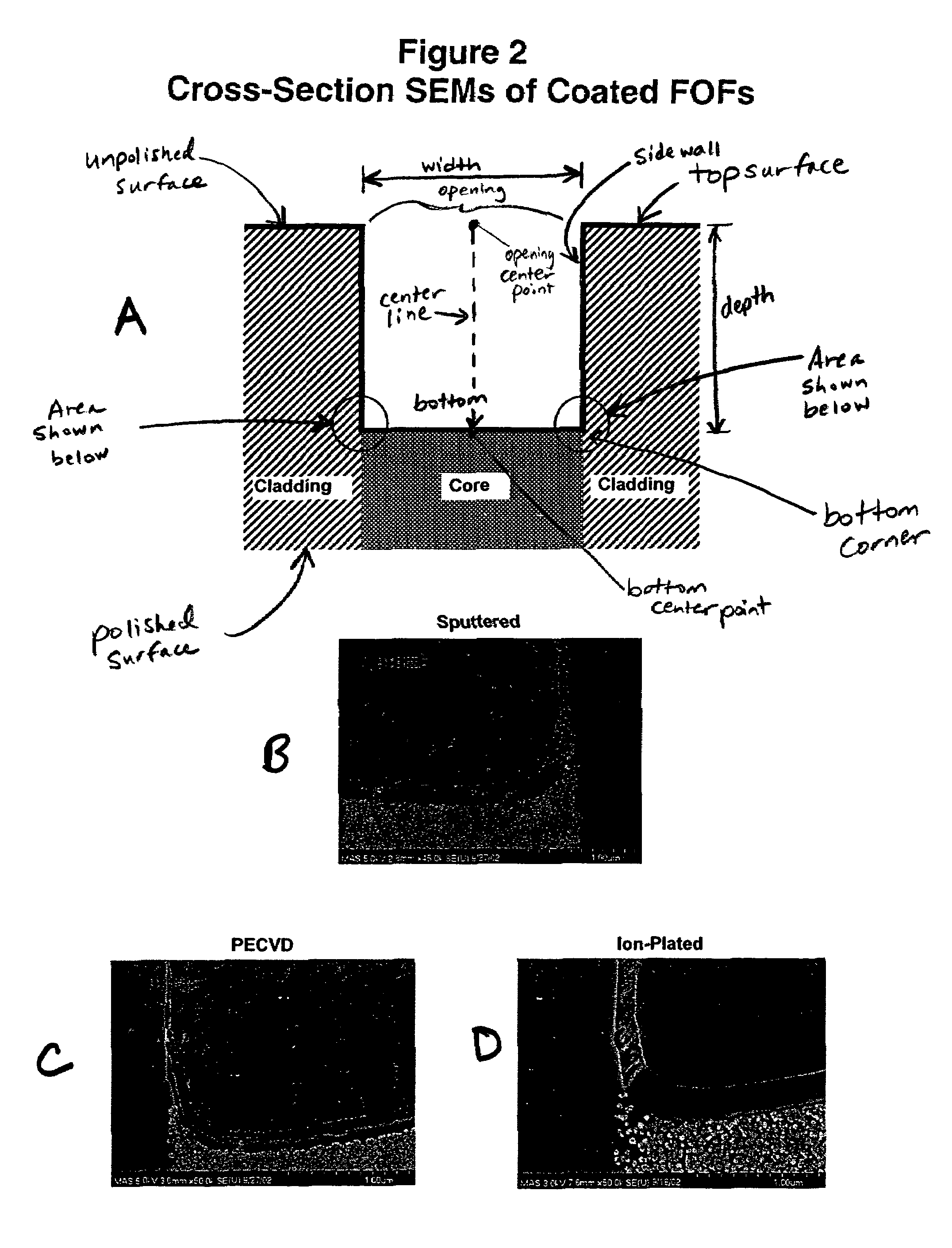
[0272]Transparent thin film coated, etched FOFs were tested for environmental robustness by exposing the etched FOF coated with SiO2 to deionized water at temperatures (approximating PCR thermal exposure), and examining SEM images of both the surfaces and cross-sections for signs of coating damage according to the following procedure. One milliliter of 1×HiFi PCR buffer (Invitrogen, Carlsbad. CA) was prepared. The thin film, etched FOF was placed on top of tissues and using a cell scraper, the excess water was removed. Quickly, 400 μL of the buffer was added on top of the FOF surface and the solution was evenly spread out with a cell scraper. After 1 minute, the excess solution was removed. The procedure of adding 400 μL of the buffer followed by removing the solution was repeated. The FOF was immediately placed in an in-house amplification device (the “AMP jig”) (454 Life Sciences, Branford, Conn.), covered wi...


PUM

PropertyMeasurementUnit
thicknessaaaaaaaaaa
thicknessaaaaaaaaaa
thicknessaaaaaaaaaa

Abstract

This invention relates to microwell array compositions which are coated with one or more thin film coatings. The invention includes the process of fabricating and using thin film coated microwell arrays.

Description

RELATED APPLICATIONS[0001]This application is a continuation in part of U.S. Ser. No. 11 / 102,075 filed on Apr. 7, 2005, the entire contents of which is hereby incorporated by reference.FIELD OF THE INVENTION[0002]This invention relates to microwell array compositions comprised of a substrate coated with one or more thin film coatings. The invention includes the process of fabricating and using the thin film coated microwell array.BACKGROUND OF THE INVENTION[0003]The ability to perform parallel microanalysis on minute quantities of sample is important to the advancement of chemistry, biology, drug discovery and medicine. Today, the traditional 1536-well microtitre plate has been surpassed by microwell arrays which have an even greater number of reaction chambers and use lesser amounts of reagents due to efforts focused on maximizing time and cost efficiencies. Although there are several types of microwell arrays available, many microwell materials prove to be incompatible with the co...

Claims


Application Information

Patent Timeline
Patent Type & Authority Patents(United States)
IPC IPC(8): C12M1/36G01N15/06H05H3/04
CPCB01L3/5085B01L2200/0668B01L2300/0819B01L2300/0822B01L2300/168G01N21/253G01N21/7703G02B6/08Y10S977/707Y10S977/702Y10S977/712
Inventor KIM, JONG-BUMLEFKOWITZ, STEVEN MARTINNOBILE, JOHNROTH, GEORGE THOMASYU, PENGGUANG
Owner 454 LIFE SCIENCES CORP
Why Eureka
Try Eureka