Thin film transistor and manufacturing method thereof

a technology of thin film transistor and manufacturing method, which is applied in the direction of basic electric elements, electrical apparatus, and semiconductor devices, can solve the problems of high manufacturing cost, inability to obtain sufficient switching characteristics, and low field-effect mobility and low on-state current, and achieve high on-state current, low off-state current, and high field-effect mobility

Inactive Publication Date: 2013-02-26
SEMICON ENERGY LAB CO LTD
View PDF25 Cites 5 Cited by
  • Summary
  • Abstract
  • Description
  • Claims
  • Application Information

AI Technical Summary

Benefits of technology

[0011]A thin film transistor whose channel region is formed using a polycrystalline silicon film features in that the field-effect mobility is far higher than those of the above-described two kinds of thin film transistors and the on-state current is high. These features enable this kind of thin film transistor to be used not only as a switching transistor in a pixel but also as an element of a driver circuit that needs to drive at high speed.
[0015]In view of the above, it is an object of an embodiment of the present invention to provide a thin film transistor which has high electric characteristics. It is an object of an embodiment of the present invention to provide a method for manufacturing a thin film transistor which has high electric characteristics with high productivity.
[0021]Further, the microcrystalline semiconductor region and the amorphous semiconductor region may include nitrogen, an NH group, or an NH2 group. Dangling bonds of semiconductor atoms which exist in the interface between microcrystalline semiconductor regions adjacent to each other (i.e., a crystal grain boundary) and the interface between the microcrystalline semiconductor region and the amorphous semiconductor region are cross-linked with an NH group, so that defect levels are reduced, which leads to formation of a path through which carriers move. A dangling bond may be terminated with an NH2 group, so that defect levels are reduced.
[0022]In the thin film transistor according to one embodiment of the present invention, the first microcrystalline semiconductor film is formed under the first condition for forming a microcrystalline semiconductor film in which a space between crystal grains is filled with an amorphous semiconductor, and the second microcrystalline semiconductor film is formed over the first microcrystalline semiconductor film under the second condition for promoting crystal growth, so that the second microcrystalline semiconductor film in which the space between crystal grains is very small and the crystallinity on a back-channel side is high can be formed, which enables the on-state current and the field-effect mobility of the thin film transistor to be increased. In addition, the amorphous semiconductor region in the semiconductor film formed over the second microcrystalline semiconductor film is a well-ordered semiconductor which has fewer defects and whose tail of a level at a band edge in the valence band is steep, which widens the band gap and suppresses the amount of tunnel current. Therefore, the amorphous semiconductor region provided between the microcrystalline semiconductor region and the impurity semiconductor film enables the off-state current of the thin film transistor to be reduced.
[0026]A thin film transistor with low off-state current, high on-state current, and high field-effect mobility can be manufactured with high productivity.

Problems solved by technology

A thin film transistor in which a channel region is formed using an amorphous silicon film has problems of low field-effect mobility and low on-state current.
On the other hand, a thin film transistor in which a channel region is formed using a microcrystalline silicon film has a problem in that, though the field-effect mobility is improved, the off-state current is higher than that of the thin film transistor whose channel region is formed using an amorphous silicon film and thus sufficient switching characteristics cannot be obtained.
However, formation of the thin film transistor whose channel region is formed using a polycrystalline silicon film involves a crystallization step for a semiconductor film and has a problem of higher manufacturing costs, as compared to formation of the thin film transistor whose channel region is formed using an amorphous silicon film.
For example, a laser annealing technique in the process for forming a polycrystalline silicon film has a problem in that large-screen liquid crystal panels cannot be produced efficiently because the area capable of being irradiated with the laser beam is small.

Method used


Image

  • Thin film transistor and manufacturing method thereof
  • Thin film transistor and manufacturing method thereof
  • Thin film transistor and manufacturing method thereof

Examples


embodiment 1

(Embodiment 1)

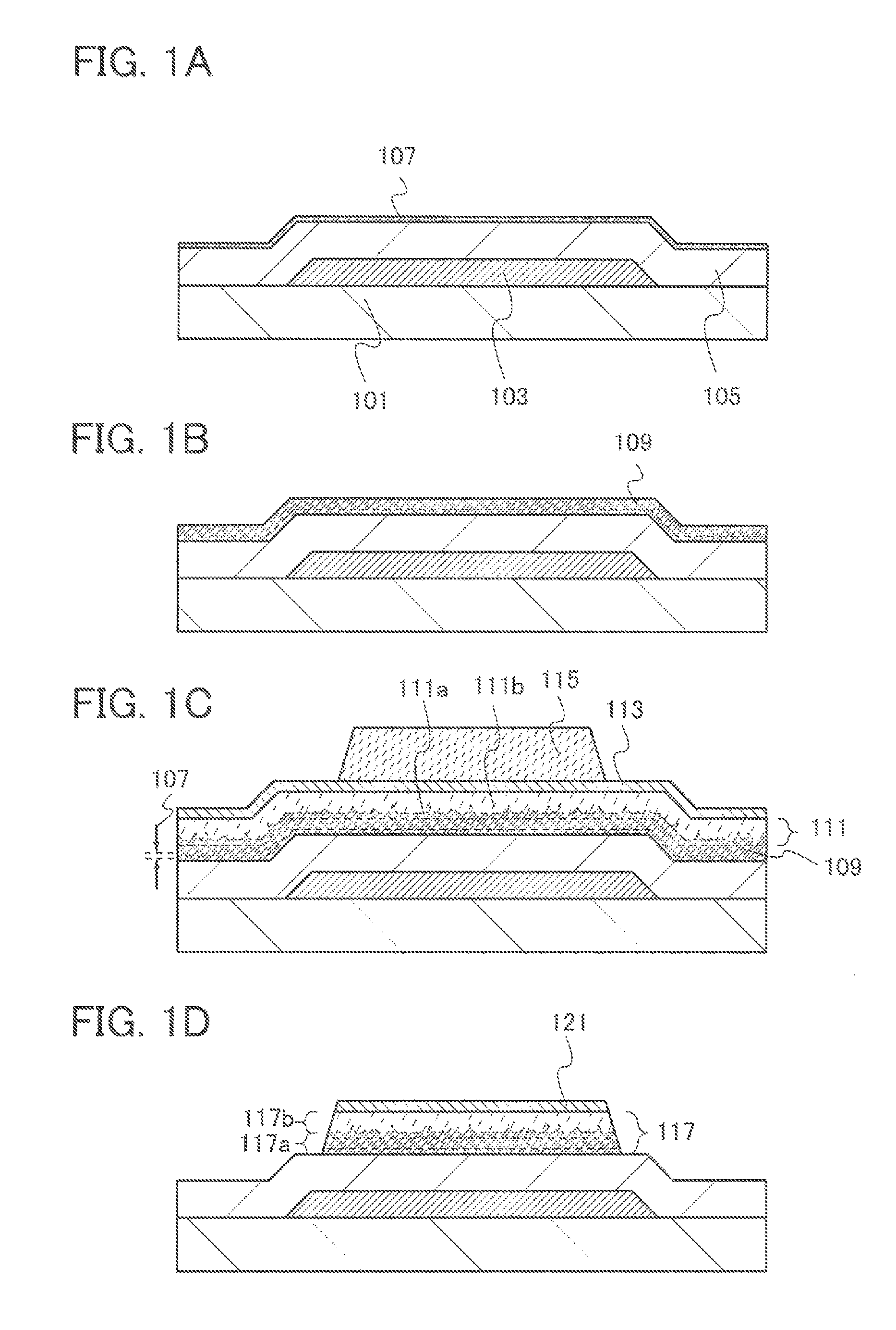
[0044]In Embodiment 1, a manufacturing method of a transistor according to one embodiment of the present invention will be described with reference to FIGS. 1A to 1D, FIGS. 2A and 2B, FIG. 3, FIGS. 4A and 4B, FIGS. 5A to 5C, and FIGS. 6A to 6D. An n-channel thin film transistor has higher carrier mobility than a p-channel thin film transistor. Further, it is preferable that all thin film transistors formed over the same substrate have the same conductivity type because the number of manufacturing steps can be reduced. Therefore, in this embodiment, a method for manufacturing an n-channel thin film transistor is described.

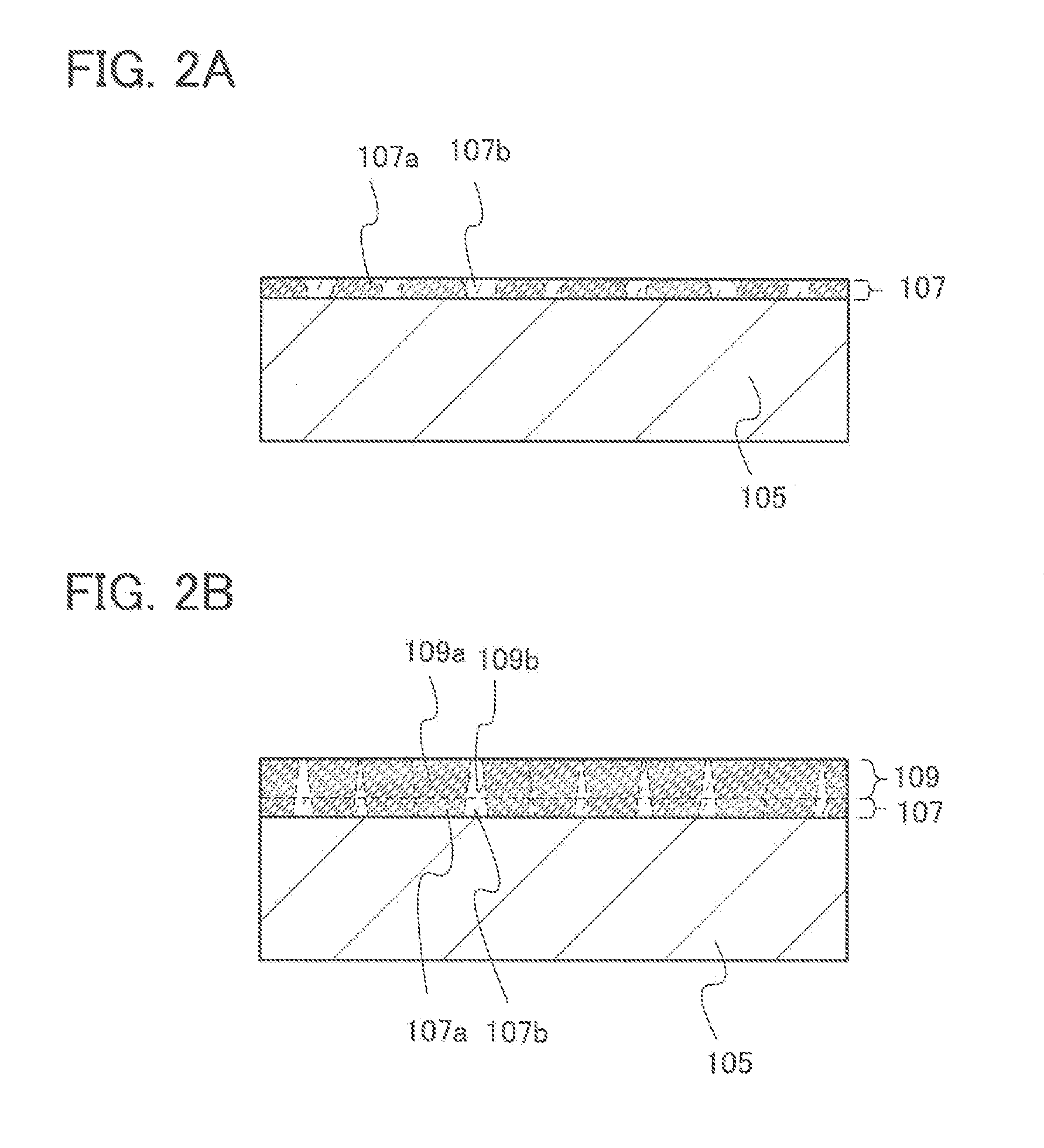
[0045]As shown in FIG. 1A, a gate electrode 103 (also called a first gate electrode) is formed over a substrate 101. Next, a gate insulating film 105 which covers the gate electrode 103 is formed, and a first microcrystalline semiconductor film 107 is formed over the gate insulating film 105.

[0046]As the substrate 101, a glass substrate; a ceramic subs...

embodiment 2

(Embodiment 2)

[0124]In Embodiment 2, a method for manufacturing a thin film transistor, by which the off-state current can be further reduced as compared to Embodiment 1 will be described with reference to FIGS. 1A to 1D and FIGS. 7A to 7C.

[0125]In a similar matter to Embodiment 1, the semiconductor stack 117 as shown in FIG. 7A is formed through the process shown in FIGS. 1A to 1C.

[0126]Next, plasma treatment is performed in which the side surface of the semiconductor stack 117 is exposed to plasma 123 with the resist mask 115 left. In Embodiment 2, plasma is generated in an oxidation gas atmosphere or a nitriding gas atmosphere, and the semiconductor stack 117 is exposed to the plasma 123. Examples of the oxidation gas include oxygen, ozone, dinitrogen monoxide, water vapor, a mixed gas of oxygen and hydrogen, and the like. Examples of the nitriding gas include nitrogen, ammonia, nitrogen fluoride, nitrogen chloride, chloroamine, fluoroamine, and the like. Plasma generation in the...

embodiment 3

(Embodiment 3)

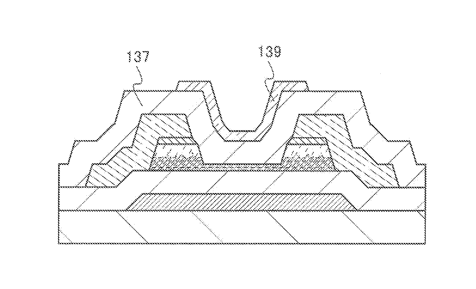
[0131]In Embodiment 3, a thin film transistor in which the off-state current can be further reduced as compared to that in the thin film transistor described in Embodiment 1 will be described with reference to FIGS. 8A to 8D.

[0132]In a similar manner to Embodiment 1, the process illustrated in FIGS. 1A to 1D and FIG. 5A is carried out, so that the conductive film 127 is formed over the gate insulating film 105 and the semiconductor stack 117. Then, as shown in FIG. 8, a mask 141 is formed using a resist by a photolithography step over the conductive film 127.

[0133]Next, as shown in FIG. 8B, the conductive film 127 and the impurity semiconductor film 121 are etched using the mask 141, so that wirings 129a and 129b which function as a source electrode and a drain electrode and a pair of impurity semiconductor films 131a and 131b which function as a source region and a drain region are formed. Further, part of an exposed portion of the amorphous semiconductor region 117b ...


PUM


Abstract

A method for manufacturing a thin film transistor having high electric characteristics with high productivity. In the method for forming a channel region of a dual-gate thin film transistor including a first gate electrode and a second gate electrode which faces the first gate electrode with the channel region provided therebetween, a first microcrystalline semiconductor film is formed under a first condition for forming a microcrystalline semiconductor film in which a space between crystal grains is filled with an amorphous semiconductor, and a second microcrystalline semiconductor film is formed over the first microcrystalline semiconductor film under a second condition for promoting crystal growth.

Description

BACKGROUND OF THE INVENTION[0001]1. Field of the Invention[0002]The present invention relates to a thin film transistor and a method for manufacturing the thin film transistor, and a display device using the thin film transistor.[0003]2. Description of the Related Art[0004]As one type of field-effect transistor, a thin film transistor whose channel region is formed using a semiconductor film which is formed over a substrate having an insulating surface is known. Techniques in which amorphous silicon, microcrystalline silicon, or polycrystalline silicon is used for the semiconductor film which is used for the channel region of the thin film transistor have been disclosed (see Patent Documents 1 to 5). A typical application of thin film transistors is a liquid crystal display television device, in which the thin film transistors are each put to practical use as a switching transistor for each pixel in a display screen.REFERENCE[0005]Patent Document 1: Japanese Published Patent Applica...

Claims


Application Information

Patent Timeline
Patent Type & Authority Patents(United States)
IPC IPC(8): H01L21/00
CPCH01L29/04H01L29/6675H01L29/66765H01L29/78618H01L29/78648H01L29/78672H01L29/78678H01L29/78696H01L29/458
Inventor ISA, TOSHIYUKI
Owner SEMICON ENERGY LAB CO LTD
Why Eureka
Try Eureka