
Atomic layer epitaxy of hematite on indium tin oxide for application in solar energy conversion

a technology of indium tin oxide and atomic layer, applied in the direction of energy input, final product manufacture, sustainable manufacturing/processing, etc., can solve the problems of limiting factors of hematite, high recombination rate of photo-generated charge carriers, and -fe/sub>2/sub>o/sub>3 /sub>may be limited by these properties, so as to improve current densities and cathodically-

Active Publication Date: 2016-07-12
UCHICAGO ARGONNE LLC
View PDF2 Cites 0 Cited by
  • Summary
  • Abstract
  • Description
  • Claims
  • Application Information

AI Technical Summary

Benefits of technology

This patent describes a method for creating thin films of a material called β-Fe2O3 by atomic layer deposition (ALD) on an epitaxial tin-doped indium oxide (ITO) template. The method allows for the growth of pure β-Fe2O3 films with a smooth and atomically sharp interface. The resulting films have improved properties such as higher current densities and cathodically-shifted onset voltages compared to films made using other methods. Additionally, the method can be used to create ultrathin Fe2O3 absorbers. The technical effect of this patent is the demonstration of a reliable method for creating high-quality β-Fe2O3 thin films with improved properties.

Problems solved by technology

However, the major limiting factors of hematite is the high recombination rate of photo-generated charge carriers combined with the relatively weak absorption of light, as well as slow water oxidation kinetics at the α-Fe2O3 surface.
While efforts have been made to improve the intrinsic charge-transport and oxidation kinetic properties of α-Fe2O3 by means of doping and surface modification, α-Fe2O3 may be limited by these properties.

Method used


Image

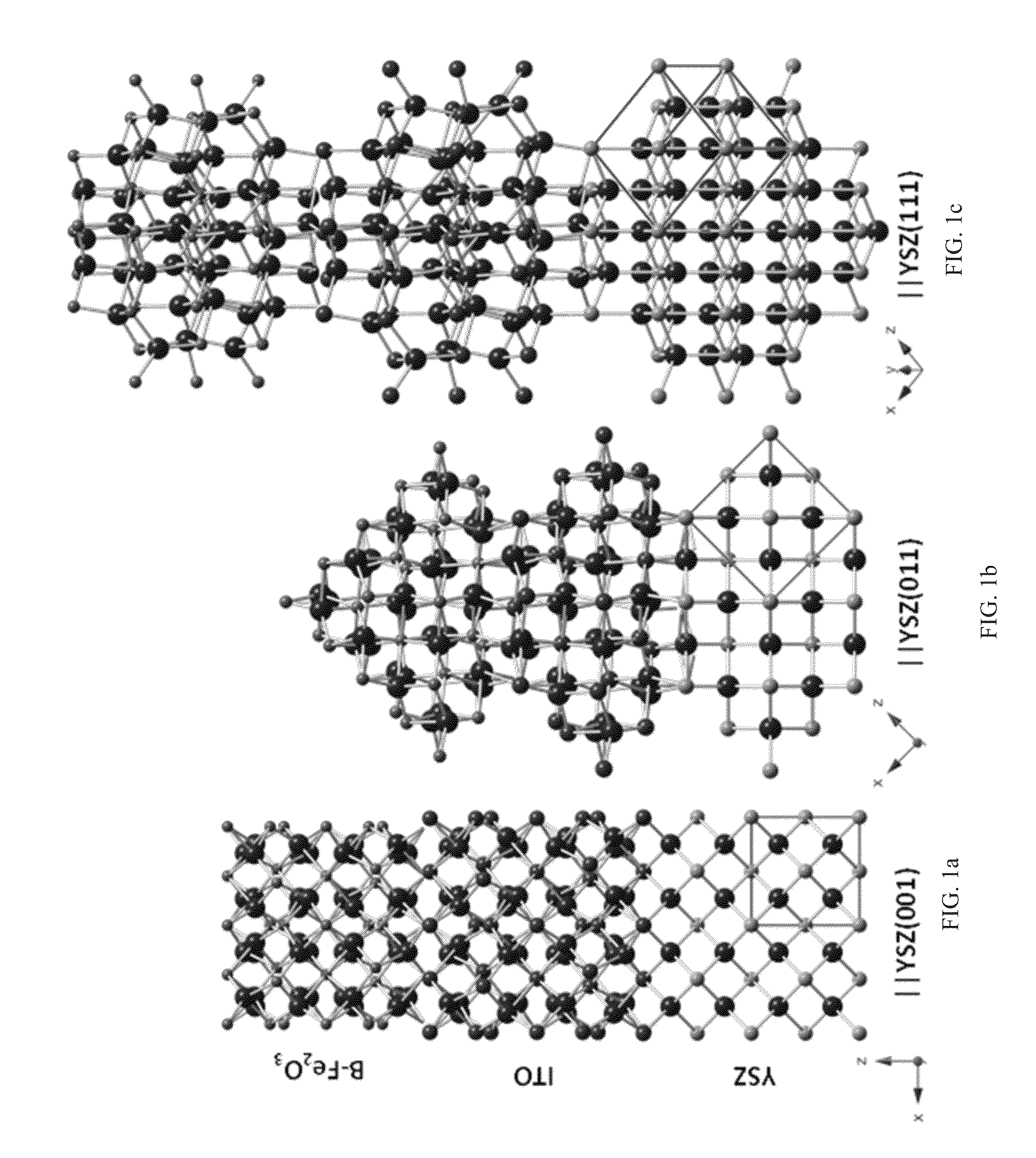
  • Atomic layer epitaxy of hematite on indium tin oxide for application in solar energy conversion
  • Atomic layer epitaxy of hematite on indium tin oxide for application in solar energy conversion
  • Atomic layer epitaxy of hematite on indium tin oxide for application in solar energy conversion

Examples


example i

[0023]Single crystal YSZ(111) samples were annealed at 1100° C. in 250 sccm high-purity O2 to obtain a smooth, terraced (100 nm) surface. Samples were then sonicated in acetone, followed by isopropyl alcohol for 10 minutes each. After each sonication the substrates were dried with N2. Samples were loaded into the ALD chamber at 250° C. and allowed to thermally equilibrate for 30 minutes before a 180 s ozone (O3) clean.

[0024]ALD was performed using a Cambridge Nanotech, Inc. Savannah 200 ALD reactor. Dose duration sequences of t1-t2-t3-t4 were used, where t1 and t3 are dose times (in seconds) for the metal and ozone precursors, respectively, while t2 and t4 are the corresponding purge times. ITO was grown based on the process developed by Elam et at [14]. Cyclopentadienylindium(I) (InCp, 99.99%, Strem) and tetrakis(dimethylamido)tin (Sn(NMe2)4, 99.99%, Aldrich) were used as metal precursors during ITO growth, and ozone was provided in 5 wt % in 100 sccm high-purity O2 using a DelOzon...

example ii

[0026]Photoelectrochemical (PEC) current-voltage measurements were performed in 0.1 M KOH (pH 13.1) using a CHI10E potentiostat. Measurement were conducted using a three electrode configuration, with Ag / AgCl and Pt as reference and counter electrodes, respectively. PEC data was normalized by the sample surface area exposed to the electrolyte (0.2 cm2). The AM1.5 solar spectrum was simulated using 300 W arc lamp, calibrated to 100 mW / cm2 using a silicon photodiode.

[0027]Raman spectra were acquired over a range of 100-1000 cm−1 using a Renishaw Ramascope spectrometer equipped with a 632.8 nm He—Ne laser. Data were collected with a 50× objective lens at 100% laser power. Collection time for each spectra was 30 s.

example iii

[0028]X-ray diffraction was used to verify the phase and epitaxial relationship between the Fe2O3 and underlying cube-on-cube ITO(111)∥YSZ(111) template. FIG. 2f presents the specular scan along the YSZ[111], where qn=4π Sin (2θ / 2) / λ, where 2θ is the scattering angle. For YSZ and ITO, only allowed reflections from the {111] families are observed. For Fe2O3, no reflections from commonly observed Fe2O3 phases (α-Fe2O3, Fe3O4) are observable (FIG. 2f).


PUM

PropertyMeasurementUnit
temperatureaaaaaaaaaa
thicknessaaaaaaaaaa
thicknessaaaaaaaaaa

Abstract

A method to provide an article of manufacture of iron oxide on indium tin oxide for solar energy conversion. An atomic layer epitaxy method is used to deposit an uncommon bixbytite-phase iron (III) oxide (β-Fe2O3) which is deposited at low temperatures to provide 99% phase pure β-Fe2O3 thin films on indium tin oxide. Subsequent annealing produces pure α-Fe2O3 with well-defined epitaxy via a topotactic transition. These highly crystalline films in the ultra thin film limit enable high efficiency photoelectrochemical chemical water splitting.

Description

STATEMENT OF GOVERNMENT RIGHTS[0001]The United States Government claims certain rights in this invention pursuant to Contract No. DE-AC02-06CH11357 between the United States Government and UChicago Argonne, LLC representing Argonne National Laboratory. The United States Government also claims certain rights in this invention pursuant to research sponsored by the Army Research Lab, ANL Cost Code 8R26900.FIELD OF THE INVENTION[0002]The invention is directed to an improved process and article of manufacture for solar energy conversion. More particularly, the invention is directed to a method to produce an atomic layer epitaxy of hematite on indium tin oxide to carry out photochemical water splitting.BACKGROUND OF THE INVENTION[0003]Of the reported phases of iron oxide, only hematite (α-Fe2O3) is considered a promising anode material for photoelectrochemical (PEC) oxidation of water for application in solar fuel production. Indeed, α-Fe2O3 possesses a suitable band gap and alignment for...

Claims


Application Information

Patent Timeline
Patent Type & Authority Patents(United States)
IPC IPC(8): C25B11/04H01G9/20C25B1/00C23C16/455C23C16/40C30B25/18C30B25/10C30B29/16C30B25/06C30B25/02
CPCC25B11/0452C23C16/406C23C16/45525C25B1/003C25B11/0405H01G9/2027Y02P20/135C30B25/02C30B25/06C30B25/10C30B25/183C30B29/16Y02P20/134Y02E10/542Y02P20/133Y02P70/50C25B1/55C25B11/051C25B11/077H10K2102/103
Inventor MARTINSON, ALEX B.RIHA, SHANNONGUO, PEIJUNEMERY, JONATHAN D.
Owner UCHICAGO ARGONNE LLC
Learn More